Combinational Logic
A combinational circuit consists of logic gates whose outputs at any time are determined from only the present combination of inputs.
A combinational circuit performs an operation that can be specified logically by a set of Boolean functions. This makes it different from "Sequential circuits" which are described below.
Sequential circuits employ storage elements in addition to logic gates. Their outputs are a function of the inputs and the state of the storage elements.
Because the state of the storage elements is a function of previous inputs. The outputs of a sequential circuit depend not only on present values of inputs but also on past inputs and the circuit behavior must be specified by a time sequence of inputs and internal states.
A combinational circuit consists of input variables, logic gates, and output variables. Combinational logic gates react to the values of the signals at their inputs and produce the value of the output signal, transforming binary information from the given input data to a required output data.
Standard combinational circuits are adders, subtractors, comparators, decoders, encoders and multiplexers.
BINARY ADDER-SUBTRACTOR
The most basic arithmetic operation is the addition of two binary digits. This simple addition consists of four possible elementary operations: 0 + 0 = 0, 0 + 1 = 1, 1 + 0 = 1, and 1 + 1 = 10
The first three operations produce a sum of one digit, but when both augend and addend bits are equal to 1. The binary sum consists of two digits. The higher significant bit of this result is called a carry.
When the augend and addend numbers contain more significant digits, The carry obtained from the addition of two bits is added to the next higher order pair of significant bits . A combinational circuit that performs the addition of two bits is called a halfadder, One that performs the addition of three bits (two significant bits and a previous carry) is a full adder. The names of the circuits stem from the fact that two half adders can be employed to implement a full adder.
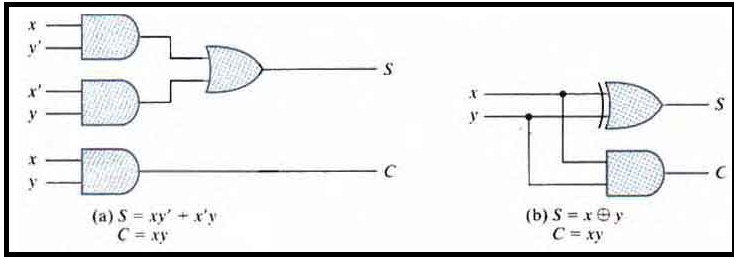
Half Adder
This circuit needs two binary inputs and two binary outputs. The input variables designate the augend and addend bits; the output variables produce the sum and carry.
We assign symbols x and y to the two inputs and S (for sum) and C ( for carry ) to the outputs.
The S output represents the least significant bit of the sum.
The simplified Boolean functions for the two outputs can be obtained directly from the truth table. The simplified sum-of-products expressions are
S = x'y + xy'
C = xy
The logic diagram of the half adder implemented in sum of products is shown. It can be also implemented with an exclusive-OR and an AND gate.
The truth table is as shown below:
| x | y | C | S |
|---|---|---|---|
| 0 | 0 | 0 | 0 |
| 0 | 1 | 0 | 1 |
| 1 | 0 | 0 | 1 |
| 1 | 1 | 1 | 0 |
Full Adder
A full adder is a combinational circuit that forms the arithmetic sum of three bits. It consists of three inputs and two outputs. Two of the input variables, denoted by x and y, represent the two significant bits to be added
The third input 'z' represents the carry from the previous lower significant position
The two outputs are designated by the symbols S for sum and C for carry. The binary variable S gives the value of the least significant bit of the sum. The binary variable C gives the output carry.
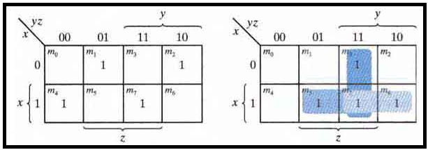
Truth table for the full adder is shown below
The boolean expression for the Sum and carry are obtained from the table as:
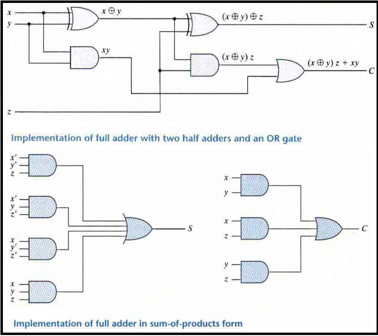
S = x ' y ' z + x'yz' + xy'z' + xyz
C = xy + xz + yz
| x | y | z | Carry | Sum |
|---|---|---|---|---|
| 0 | 0 | 0 | 0 | 0 |
| 0 | 0 | 1 | 0 | 1 |
| 0 | 1 | 0 | 0 | 1 |
| 0 | 1 | 1 | 1 | 0 |
| 1 | 0 | 0 | 0 | 1 |
| 1 | 0 | 1 | 1 | 0 |
| 1 | 1 | 0 | 1 | 0 |
| 1 | 1 | 1 | 1 | 1 |
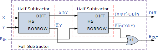
Full adder using two half adders
Full adder can also be implemented with two half adders and one OR gate.
The S output from the second half adder is the exclusive-OR of z and the output of the first half adder giving
S = z ⊕ (x ⊕ y)
= z'(xy' + x'y) + z(xy' + x' y)'
= z'(xy' + x'y) + z(xy + x'y')
= xy'z' + x'yz' + xyz + x'y'z
C = z(xy' + x'y) + xy = xy'z + x'yz + xy
Binary Adder
A binary adder is a digital circuit that produces the arithmetic sum of two binary numbers. It can be constructed with full adders connected in cascade. with the output carry from each full adder connected to the input carry of the next full adder in the chain.
An n-bit adder requires n full adders with each output carry connected to the input carry of the next higher order full adder
The bits are added with full adders starting from the least significant position (subscript 0) to form the sum bit and carry bit. The input carry C0 in the least significant position must be 0. The value of Ci+1 in a given significant position is the output carry of the full adder. This value is transferred into the input carry of the full adder that adds the bits one higher significant position to the left.
The sum bits are thus generated starting from the rightmost position and are available as soon as the corresponding previous carry bit is generated. All the carries must be generated for the correct sum bits to appear at the outputs.
Carry Propagation
The addition of two binary numbers in parallel implies that all the bits of the augend and addend are available for computation at the same time.
However this is not the case since longest propagation delay time in an adder is the time it takes the carry to propagate through the full adders. Since each bit of the sum output depends on the value of the input carry the value of Sj - (Sum of bits at positon 'j') at any given stage in the adder will be in its steady-state final value only after the input carry to that stage has been propagated.
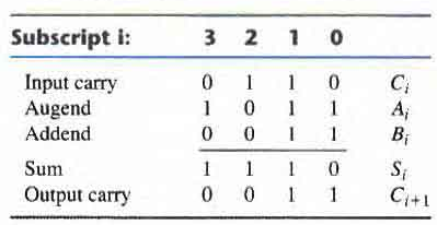
Consider in a four bit adder we have Inputs A3 and B3 are available as soon as input signals are applied to the adder. However, input carry C3 does not settle to its final value until C2 is available from the previous stage. Similarly, C2 has to wait for C1 and so on down to C0. Thus, only after the carry propagates and ripples through all stages will the last output S3 and carry C4 settle to their final correct value.
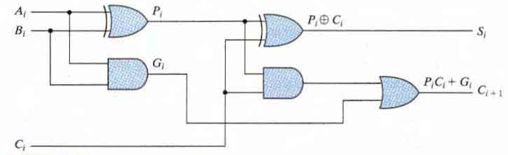
The above figure shows a full adder circuit which would at stage 'i' of the binary adder. The diagram shows clearly that for Pi and Gi there is no need for overhead. However overhead occurs for calculation of Sum and carry as previous carry has to pass through AND and OR gate at the second level to get the output.
Thus, If there are four full adders in the adder then output carry C4 would have to pass through 2*4=8 gate levels from C0 to C4.
For an n-bit adder, there '2n' gate levels to propagate from input to output.
The carry propagation time is an important attribute of the adder because it limits the speed with which two numbers are added. Although the adder or for that matter any combinational circuit will always have some value at its output terminals, the outputs will not be correct unless the signals are given enough time to propagate through the gates connected from the inputs to the outputs.
There are several techniques for reducing the carry propagation time in a parallel adder. The most widely used technique employs the principle of carry lookahead logic.
Carry Look-ahead Generator
From the diagram of the full adder circuit shown above we obtain two variables Pi and Gi which are defined as:
Pi = Ai ⊕ Bi
Gi = Ai . Bi
the output sum and carry can be expressed as:
Si = Pi ⊕ Ci
Ci+1 = Gi + PiCi
Gi is called a carry generate and it produces a carry of 1 when both Ai and Bi are 1, regardless of the input carry Ci, Pi is called a Carry Propagate, because it determines whether a carry into stage 'i' will propagate into stage i+1 (i.e whether an assertion of Ci will propagate to an assertion of Ci+1.
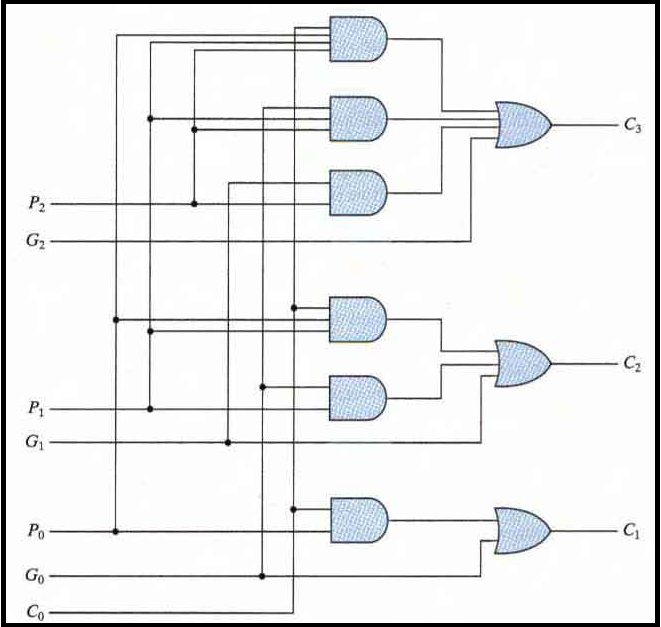
Boolean functions for the carry outputs of each stage and substitute the value of each Ci from the previous equations:
C0 = input carry
C1 = G0 + P0C0
C2 = G1 + P1C1 = G1 + P1(G0 + P0C0) = G1 + P1G0 + P1P0C0
C3 = G2 + P2C2 = G2 + P2G1 + P2P1G0 = P2P1P0C0
Since the Boolean function for each output carry is expressed in sum-of-products form each function can be implemented with one level of AND gates followed by an OR gate (or by a two-level NAND)
The three Boolean functions for C1, C2 and C3 are implemented in the carry lookahead generator shown below. Note that this circuit can add in less time because C3 does not have to wait for C2 and C1 to propagate, in fact C3 is propagated at the same time as C1 and C2. Thus gain in speed of operation is achieved at tbe expense of additional complexity (hardware).
Each sum output requires two exclusive-OR gates. The output of the first exclusive-OR gate generates the Pi variable, and the AND gate generates the Givariable. The carries are propagated through the carry lookahead generator and applied as inputs to the second exclusive-OR gate
All output carries are generated after a delay through two levels of gates. Thus, outputs S1 through S3 have equal propagation delay times.
Binary Adder - Subtractor
The subtraction of unsigned binary numbers can be done most conveniently by means of complements. The subtraction A - B can be done by taking the 2's complement of B and adding it to A. The 2' s complement can be obtained by taking the 1's complement and adding 1 to the least significant pair of bits. The 1's complement can be implemented with inverters and a 1 can be added to the sum through the input carry.
It is worth noting that binary numbers in the signed-complement system are added and subtracted by the same basic addition and subtraction rules as are unsigned numbers. Therefore computers need only one common hardware circuit to handle both types of arithmetic. The user or programmer must interpret the results of such addition or subtraction differently depending on whether it is assumed that the numbers are signed or unsigned.
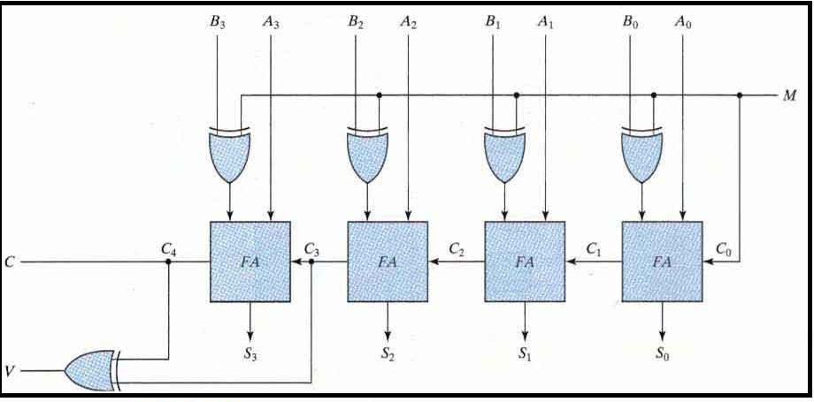
The addition and subtraction operations can be combined into one circuit with one common binary adder by including an exclusive-OR gate with each full adder.
The mode input M controls the operation.
When M = 0 the circuit is an adder and When M=1 the circuit becomes a subtracter.
Each exclusive-OR gate receives input M and one of the inputs of B. When M = 0 we have B ⊕ 0 = B. The full adders receive the value of B the input carry is 0 and the circuit performs A plus B.
When M = 1, we have B ⊕ 1 = B' and C0 = 1. The B inputs are all complemented and a 1 is added through the input carry. The circuit performs the operation A plus the 2' s complement of B. (The ex clusive-OR with output V is for detecting an overflow)
The circuit for subtracting A - B consists of an adder with inverters placed between each data input B and the corresponding input of the full adder. The input carry C0 must be equal to 1 when subtraction is performed. The operation thus performed becomes A plus the 1's complement of B plus 1.
This is equal to A plus the 2' s complement of B. For unsigned numbers that gives A - B if A ≥ B or the 2's complement of ( B - A ) if A < B. For signed numbers the result is A - B, provided that there is no overflow
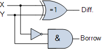
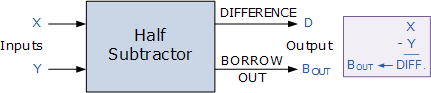
Half Subtractor
A half subtractor is a logical circuit that performs a subtraction operation on two binary digits. The half subtractor produces a difference and a borrow bit for the next stage.
Truth table of Half Subtractor :
From the truth table of the half subtractor we can see that the DIFFERENCE (D) output is the result of the Exclusive-OR gate and the Borrow-out (Bout) is the result of the NOT-AND combination
Then the Boolean expression for a half subtractor is as follows.
D = X XOR Y = X ⊕ Y
B = not-X AND Y = X.Y
Half Subtractor circuit :
Half Subtractor block diagram :
| y | x | Difference | Borrow |
|---|---|---|---|
| 0 | 0 | 0 | 0 |
| 0 | 1 | 1 | 0 |
| 1 | 0 | 1 | 1 |
| 1 | 1 | 0 | 0 |
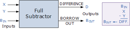
Full Subractor :
A full subtractor has three inputs. The two single bit data inputs X (minuend) and Y (subtrahend) the same as before plus an additional Borrow-in (B-in) input to receive the borrow generated by the subtraction process from a previous stage.
Full subractor circuit diagram :
Full subractor logic diagram :
Full subractor truth table :
Then the Boolean expression for a full subtractor is as follows.
DIFFERENCE (D) : (X ⊕ Y) ⊕ BIN
BORROW OUT (BOUT) : X . Y = (X ⊕ Y)BIN
| B-in | y | x | Difference | Borrow |
|---|---|---|---|---|
| 0 | 0 | 0 | 0 | 0 |
| 0 | 0 | 1 | 1 | 0 |
| 0 | 1 | 0 | 1 | 1 |
| 0 | 1 | 1 | 0 | 0 |
| 1 | 0 | 0 | 1 | 1 |
| 1 | 0 | 1 | 0 | 0 |
| 1 | 1 | 0 | 0 | 1 |
| 1 | 1 | 1 | 1 | 1 |