Synchronous Sequential Logic
Although every digital system is likely to have some combinational circuits, most systems encountered in practice also include storage elements which require that the system can be described in terms of sequential logic.
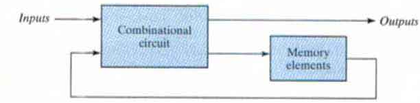
Sequential Logic consists of combinational circuit to which storage elements are connected to form a feedback path.
Storage elements are devices capable of storing binary information. This information that is stored at any time defines the state of the sequential circuit at that time.
The sequential circuit receives binary valued inputs from external sources, this together with the present state of the storage elements determines the binary value of the outputs.
These external inputs also determine the condition for changing the state in the storage elements.
The block diagram demonstrates that the outputs in a sequential circuit are a function not only of the inputs, but also of the present state of the storage elements.
The next state of the storage elements is also a function of external inputs and the present state. Thus, a sequential circuit is specified by a time sequence of inputs, outputs, and internal states.
There are two main types of sequential circuits, and their classification is a function of the timing of their signals.
Asynchronous sequential circuit: A system whose behavior depends upon the input signals at any instant of time and the order in which the inputs change, The storage elements commonly used in asynchronous sequential circuits are time-delay devices.
Synchronous sequential circuit: A system whose behavior can be defined from the knowledge of its signals at discrete instants of time. They use a clock pulse for controlling the output.
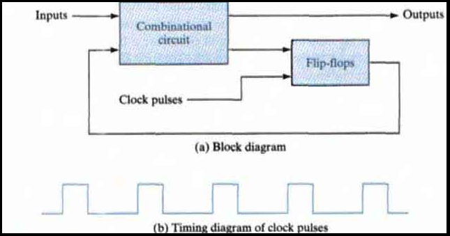
Synchronous sequential circuit employs signals that affect the storage elements at only discrete instants of time. Synchronization is achieved by a timing device called a 'a clock generator', which provides a clock signal having the form of a periodic train of 'clock pulses'.
The clock pulses are distributed throughout the system in such a way that storage elements are affected only with the arrival of each pulse.
The clock pulses determine when computational activity will occur within the circuit, and other signals (external inputs and otherwise) determine what changes will take place affecting the storage elements and the outputs.
Example, a circuit that is to add and store two binary numbers would compute their sum from the values of the numbers and store the sum at the occurrence of a clock pulse.
Synchronous sequential circuits that use clock pulses to control storage elements are called clocked sequential circuits and are the type most frequently encountered in practice.
They are called synchronous circuits because the activity within the circuit and the resulting updating of stored values is synchronized to the occurrence of clock pulses.
Advantage of Synchronous circuits:
The design of synchronous circuits is feasible because they seldom manifest instability problems
Their timing is easily broken down into independent discrete steps, each of which can be considered separately.
Block diagram - Synchronous clocked sequential circuit
The storage elements (memory) used in clocked sequential circuits are called flip-flops. A flip-flop is a binary storage device capable of storing one bit of information. In a stable state, the output of a flip-flop is either 0 or 1.
The outputs are formed by a combinational logic function of the inputs to the circuit or the values stored in the flip-flops (or both).
The value that is stored in a flip-flop when the clock pulse occurs is also determined by the inputs to the circuit or the values presently stored in the flip-flop or both.
The new value is stored (i.e the flip-flop is updated) when a pulse of the clock signal occurs. Prior to the occurrence of the clock pulse the combinational logic forming the next value of the flop-flop must have reached a stable value.
The transition from one state to the next occurs only at predetermined intervals dictated by the clock pulse - value of the clock signals changes from 0 to 1 or 1 to 0.
STORAGE ELEMENTS : LATCHES
A storage element in a digital circuit can maintain a binary state indefinitely (as long as power is delivered to the circuit), until directed by an input signal to switch states.
The major differences among various types of storage elements are in the number of inputs they possess and in the manner in which the inputs affect the binary state.
Storage elements that operate at signal levels are referred to as latches; Those controlled by clock transitions are called flipflops.
Latches are level sensitive and Flipflops are edge sensitive.
Although latches are useful for storing binary information and for the design of asynchronous sequential circuits but they are not practical for use in synchronous sequential circuits.
They are however the building blocks of flip-flops
SR Latch
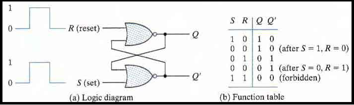
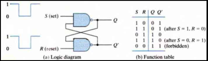
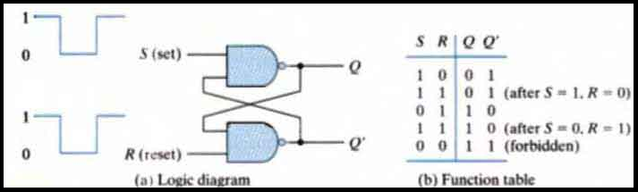
The SR latch is a circuit with two cross-coupled NOR gates or two cross-coupled NAND gates and two inputs labeled S for set and R for reset.
The latch has two useful states:
When output Q = 1 and Q' = 0 the latch is said to be in the set state
When Q = 0 and Q' = 1 it is in the reset state
Outputs Q and Q' are normally the complement of each other. However. when both inputs are equal to 1 at the same time, a condition in which both outputs are equal to 0 (rather than be mutually complementary) occurs.
If both inputs are then switched to 0 simultaneously, the device will enter an unpredictable or undefined state or a metastable state. Consequently, in practical applications setting both inputs to 1 is forbidden .
Under normal conditions both inputs of the latch remain at 0 unless the state has to be changed
SR Latch using Cross coupled NOR Gates
Both inputs of the latch remain at 0 unless the state has to be changed. The application of a momentary 1 to the S input causes the latch to go to the set state.
The S input must go back to 0 before any other changes take place , in order to avoid the occurrence of an undefined next state that results from the forbidden input condition.
Now, two input conditions cause the circuit to be in the set state.
The first condition (S = 1, R = 0) is the action that must be taken by input S to bring the circuit to the set state. Removing the active input from S leaves the circuit in the same state.
After both inputs return to 0, it is then possible to shift to the reset state by momentary applying a 1 to the R input. The 1 can then be removed from R, whereupon the circuit remains in the reset state.
Thus, when both inputs S and R are equal to 0, the latch can be in either the set or the reset state. depending on which input was most recently a 1.
If a 1 is applied to both the S and R inputs of the latch both outputs go to 0. This action produces an undefined next state because the state that results from the input transitions depends on the order in which they return to 0.
It also violates the requirement that outputs be the complement of each other. In normal operation this condition is avoided by making sure that 1' s are not applied to both inputs simultaneously.
SR latch with two cross-coupled NAND gates
It operates with both inputs normally at 1 unless the state of the latch has to be changed
The application of 0 to the S input causes output Q to go to 1 putting, the latch in the Set state. When the S input goes back to 1 the circuit remains in the set state.
After both inputs go back to 1 we are allowed to change the state of tbe latch by placing a 0 in the R input.
This action causes the circuit to go to the reset state and stay there even after both inputs return to 1.
The condition that is forbidden for the NAND latch is both inputs being equal to 0 at the same time, an input combination that should be avoided.
In comparing the NAND with the NOR latch, note that the input signals for the NAND require the complement of those values used for the NOR latch.
Hence a NAND latch is also called a S'R' latch.
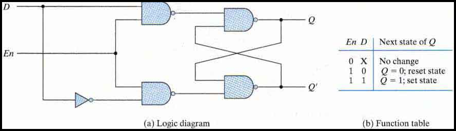
In an SR Latch an additional input called control input can be provided to decide when the state of the latch can be changed.
It consists of the basic SR latch and two additional NAND gates
SR Latch with control inputs
The control input En acts as a enable for the other two inputs.
The output of the NAND gates stay at logic 1 level as long as the enable signal remains at 0.
When the enable signal goes to 1, the S and R are allowed affect the latch.
The set state is reached when S = 1, R = 0 and En = 1
The reset state is reached when S = 0, R = 1 and En = 1
In either case, when En returns to 0, the circuit remains in its current state
The control input disables the circuit by applying 0 to En so that the state of the output does not change regardless of the values of S and R. Moreover when En = 1 and both the S and R inputs are equal to 0 the state of the circuit does not change.
An indeterminate condition occurs when all three inputs are equal to 1. This condition places 0's on both inputs of the basic SR latch, which puts it in the undefined state.
When the enable input goes back to 0, one cannot conclusively determine the next state because it depends on whether the S or R input goes to 0 first.
This indeterminate condition makes this circuit difficult to manage and it is seldom used in practice.
D Latch (Transparent Latch)
This latch has only two inputs: D (data) and En (enable). The D input goes directly to the S input and its complement is applied to the R input.
One way to eliminate the undesirable condition of the indeterminate state in the SR latch is to ensure that inputs S and R are never equal to 1 at the same time. This is done in the D latch.
As long as the enable input is at 0, the cross-coupled SR latch has both inputs at the 1 level and the circuit cannot change state regard less of the value of D.
The D input is sampled when En = 1, If D = 1, the Q output goes to 1 placing the circuit in the set state. If D = 0 output Q goes to 0 placing the circuit in the reset state.
The D latch receives that designation from its ability to hold data in its internal storage.
Properties of D - Latch
It is suited for use as a temporary storage for binary information between a unit and its environment
The binary information present at the data input of the D latch is transferred to the Q output when the enable input is asserted. The output follows changes in the data input as long as the enable input is asserted. This situation provides a path from input D to the output and for this reason the circuit is often called a transparent latch.
When the enable input signal is deasserted the binary information that was present at the data input at the time the transition occurred is retained (i.e. stored) at the Q output until the enable input is asserted again.