Registers and Counters
A clocked sequential circuit consists of a group of flip-flops and combinational gates connected to form a feedback path. The flip-flops are essential because in their absence the circuit reduces to a purely combinational circuit.
A circuit with flip-flops is considered a sequential circuit even in the absence of combinational gates.
A register is a group of flip-flops each one of which is capable of storing one bit of information. An n-bit register consists of a group of 'n' flip-flops capable of storing 'n' bits of binary information.
A Counter is essentially a register that goes through a predetermined sequence of binary states. The gates in the counter are connected in such a way as to produce the prescribed sequence of states.
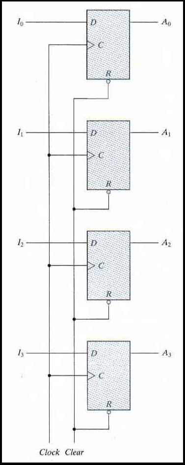
Simple Register
A register constructed with four D-type flip-flops is shown below to form a four-bit data storage register.
The common clock input triggers all flip-flops on the positive edge of each pulse, and the binary data available at the four inputs are transferred into the register.
The four outputs can be sampled at any time to obtain the binary information stored in the register. The input Clear_b goes to the active-low R (reset) input of all four flip-flops
When this input goes to 0, all flip-flops are reset asynchronously.
The Clear_b input is useful for clearing the register to all 0's prior to its clocked operation. The R inputs must be maintained at logic 1 during normal clocked operation
Note that, depending on the flip-flop either Clear, Clear_b, reset or reset_b can be used to indicate the transfer of the register to an all 0's state
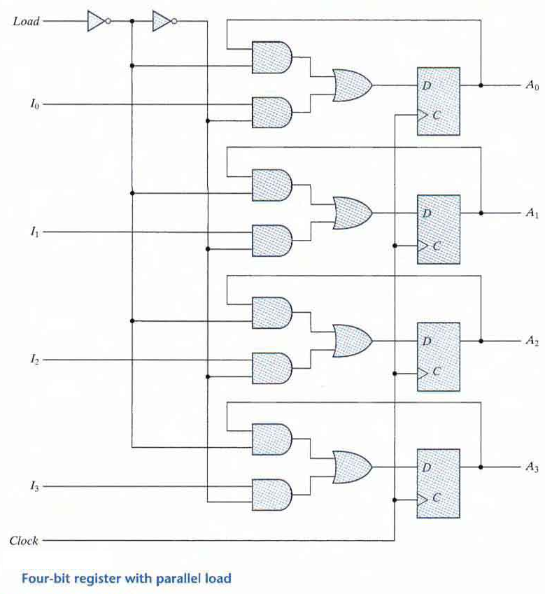
Register with Parallel Load
Synchronous digital systems have a master clock generator that supplies a continuous train of clock pulses.
The pulses are applied to all flip-flops and registers in the system.
A separate control signal must be used to decide which register operation will execute at each clock pulse.
The transfer of new information into a register is referred to as loading or updating the register. If all the bits of the register are loaded simultaneously with a common clock pulse, we say that the loading is done in parallel.
A clock edge applied to the C inputs of the register will load all four inputs in parallel.
If the contents of the register must be left unchanged the inputs must be held constant or the clock must be inhibited from the circuit.
A four-bit data-storage register with a load control input that is directed through gates and into the D inputs of the flip-flops is shown below.
The additional gates implement a two channel mux whose output drives the input to the register with either the data bus or the output of the register. The load input to the register determines the action to be taken with each clock pulse.
When the load input is 1 the data at the four external inputs are transferred into the register with the next positive edge of the clock. When the load input is 0 the outputs of the flip-flops are connected to their respective inputs.
The feedback connection from output to input is necessary because a D flip-flop does not have a "no change" condition. With each clock edge the D input determines the next state of the register
To leave the output unchanged it is necessary to make the D input equal to the present value of the output i.e. the output circulates to the input at each clock pulse. The clock pulses are applied to the C in puts without interruption.
The load input determines whether the next pulse will accept new information or leave the information in the register intact.
The transfer of information from the data inputs or the outputs of the register is done simultaneously with all four bits in response to a clock edge.
SHIFT REGISTERS
A register capable of shifting the binary information held in each cell to its neighboring cell, in a selected direction is called a shift register.
The logical configuration of a shift register consists of a chain of flip-flops in cascade with the output of one flip-flop connected to the input of the next flip-flop. All flip-flops receive common clock pulses, which activate the shift of data from one stage to the next.
The simplest possible shift register is one that uses only flip-flops, as shown below. The output of a given flip-flop is connected to the D input of the flip-flop at its right. This shift register is unidirectional.
Each clock pulse shifts the contents of the register one bit position to the right. The configuration does not support a left shift.
The serial input determines what goes into the leftmost flip-flop during the shift. The serial output is taken from the output of the rightmost flip-flop.
Serial Transfer
A digital system is said to operate in serial mode when information is transferred and manipulated one bit at a time. Information is transferred one bit at a time by shifting the bit out of the source register and into the destination register.
This type of transfer is in contrast to parallel transfer whereby all the bits of the register are transferred at the same time.
The serial output (SO) of first register is connected to the serial input (SI) of second register. To prevent the loss of information stored in the source register, the information in the first register is made to circulate by connecting the serial output to its serial input.
The initial content of the second register is shifted out through its serial output and is lost unless it is transferred to a third shift register. The shift control input determines when and how many times the registers are shifted.
Operation of Shift Registers:
Suppose the shift registers have four bits each. Then the control unit that supervises the transfer of data must be designed in such a way that it enables the shift registers through the shift control signal for a fixed time of four clock pulses
The shift control signal is synchronized with the clock and changes value just after the negative edge of the clock.
The next four clock pulses find the shift control signal in the active state so the output of the AND gate connected to the Clk inputs produces four pulses: T1, T2, T3, T4.
Each rising edge of the pulse causes a shift in both registers. The fourth pulse changes the shift control to 0, and the shift registers are disabled.