Combinational Circuits
A combinational circuit is a connected arrangement of logic gates with a set of inputs and outputs. At any given time, the binary values of the outputs are a function of the binary combination of the inputs.
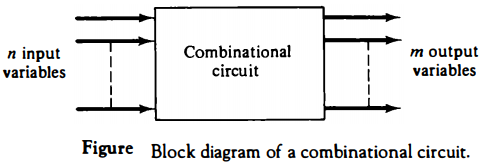
A block diagram of a combinational circuit is shown in Fig. below.
The n binary input variables come from an external source, the m binary output variables go to an external destination, and in between there is an interconnection of logic gates.
A combinational circuit transforms binary information from the given input data to the required output data. Combinational circuits are employed in digital computers for generating binary control decisions and for providing digital components required for data processing.
A combinational circuit can be described by a truth table showing the binary relationship between the n input variables and the m output variables. The truth table lists the corresponding output binary values for each of the 2n input combinations.
A combinational circuit can also be specified with m Boolean functions, one for each output variable. Each output function is expressed in terms of the n input variables
The analysis of a combinational circuit starts with a given logic circuit diagram and culminates with a set of Boolean functions or a truth table. If the digital circuit is accompanied by a verbal explanation of its function, the Boolean functions or the truth table is sufficient for verification.
If the function of the circuit is under investigation, it is necessary to interpret the operation of the circuit from the derived Boolean functions or the truth table.
The success of such investigation is enhanced if one has experience and familiarity with digital circuits.
The ability to correlate a truth table or a set of Boolean functions with an information-processing task is an art that one acquires with experience. The design of combinational circuits starts from the verbal outline of the problem and ends in a logic circuit diagram. The procedure involves the following steps:
1. The problem is stated.
2. The input and output variables are assigned letter symbols.
3. The truth table that defines the relationship between inputs and outputs
is derived.
4. The simplified Boolean functions for each output are obtained.
5. The logic diagram is drawn.
Half-Adder
The most basic digital arithmetic circuit is the addition of two binary digits.
A combinational circuit that performs the arithmetic addition of two bits is called a half-adder.
One that performs the addition of three bits (two significant bits and a previous carry) is called a full-adder.
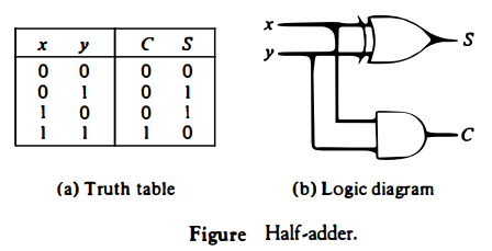
The name of the former stems from the fact that two half-adders are needed to implement a full-adder. The input variables of a half-adder are called the augend and addend bits. The output variables the sum and carry.
It is necessary to specify two output variables because the sum of 1 + 1 is binary 10, which has two digits. We assign symbols x and y to the two input variables, and S (for sum) and C (for carry) to the two output variables.
The truth table for the half-adder is shown in Fig. below.
The C output is 0 unless both inputs are 1. The S output represents the least significant bit of the sum.
The Boolean functions for the two outputs can be obtained directly from the truth table: S = x'y + xy' = x ⊕ y c = xy
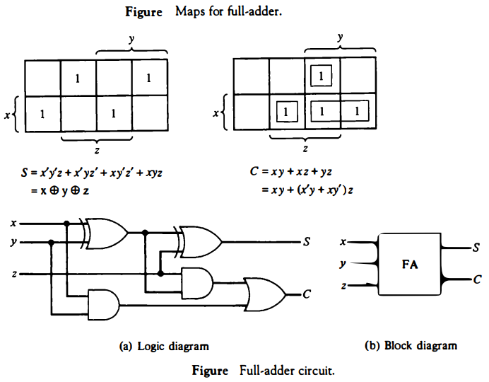
Full-Adder
A full-adder is a combinational circuit that forms the arithmetic sum of three input bits. It consists of three inputs and two outputs. Two of the input variables, denoted by x and y, represent the two significant bits to be added. The third input, z, is the carry from the previous lower significant position.
The two outputs are designated by the symbols S (for sum) and C (for carry). The binary variable S gives the value of the least significant bit of the sum. The binary variable C gives the output carry.
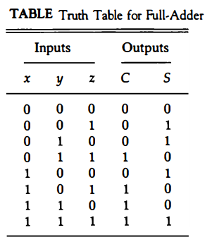
The maps of Fig. below are used to find algebraic expressions for the two output variables. The 1's in the squares for the maps of S and C are determined directly from the minterms in the truth table
The squares with 1's for the S output do not combine in groups of adjacent squares. But since the output is 1 when an odd number of inputs are 1, S is an odd function and represents the exclusive-OR relation of the variables
One possible expression for C is C = xy + (x'y + xy')z
Realizing that x'y + xy' = x ⊕ y and including the expression for output S, we obtain the two Boolean expressions for the full-adder: S=x ⊕ y ⊕ z C = xy + (x ⊕ y)z
Flip-Flops
The digital circuits considered thus far have been combinational, where the outputs at any given time are entirely dependent on the inputs that are present at that time.
Although every digital system is likely to have a combinational circuit, most systems encountered in practice also include storage elements, which require that the system be described in terms of sequential circuits.
The most common type of sequential circuit is the synchronous type
. Synchronous sequential circuits employ signals that affect the storage elements only at discrete instants of time.
Synchronization is achieved by a timing device called a clock pulse generator that produces a periodic train of clock pulses. The clock pulses are distributed throughout the system in such a way that storage elements are affected only with the arrival of the synchronization pulse.
Clocked synchronous sequential circuits are the type most frequently encountered in practice. They seldom manifest instability problems and their timing is easily broken down into independent discrete steps, each of which may be considered separately.
The storage elements employed in clocked sequential circuits are called flip-flops. A flip-flop is a binary cell capable of storing one bit of information.
It has two outputs, one for the normal value and one for the complement value of the bit stored in it. A flip-flop maintains a binary state until directed by a clock pulse to switch states.
The difference among various types of flip-flops is in the number of inputs they possess and in the manner in which the inputs affect the binary state
SR Flip-Flop
It has three inputs, labeled S (for set), R (for reset), and C (for clock).
It has an output Q and sometimes the flip-flop has a complemented output, which is indicated with a small circle at the other output terminal.
There is an arrowhead-shaped symbol in front of the letter C to designate a dynamic input.
The dynamic indicator symbol denotes the fact that the flip-flop responds to a positive transition (from 0 to 1) of the input clock signal .
The operation of the SR flip-flop is as follows :
If there is no signal at the clock input C, the output of the circuit cannot change irrespective of the values at inputs S and R.
Only when the clock signal changes from 0 to 1 can the output be affected according to the values in inputs S and R.
If S = 1 and R = 0 when C changes from 0 to 1, output Q is set to 1.
If S = 0 and R = 1 when C changes from 0 to 1, output Q is cleared to 0.
If both S and R are 0 during the clock transition, the output does not change.
When both S and R are equal to 1, the output is unpredictable and may go to either 0 or 1, depending on internal timing delays that occur within the circuit.
The characteristic table shown in Fig. below summarizes the operation of the SR flip-flop in tabular form.
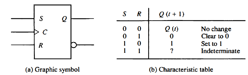
The S and R columns give the binary values of the two inputs .
Q(t) is the binary state of the Q output at a given time (referred to as present state). Q(t + 1) is the binary state of the Q output after the occurrence of a clock transition (referred to as next state).
If S = R = 0, a clock transition produces no change of state [i.e., Q(t + 1) = Q(t)] .
If S = 0 and R = 1, the flip-flop goes to the 0 (clear) state. If S = 1 and R = 0, the flip-flop goes to the 1 (set) state.
The SR flip-flop should not be pulsed when S = R = 1 since it produces an indeterminate next state . This indeterminate condition makes the SR flip-flop difficult to manage and therefore it is seldom used in practice.
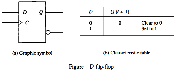
D Flip-Flop
The D (data) flip-flop is a slight modification of the SR flip-flop.
An SR flip-flop is converted to a D flip-flop by inserting an inverter between S and R and assigning the symbol D to the single input.
The D input is sampled during the occurrence of a clock transition from 0 to 1.
If D = 1, the output of the flip-flop goes to the 1 state, but if D = 0, the output of the flip-flop goes to the 0 state .
From the characteristic table we note that the next state Q(t + 1) is determined from the D input. The relationship can be expressed by a characteristic equation: Q(t + 1) = D
This means that the Q output of the flip-flop receives its value from the D input every time that the clock signal goes through a transition from 0 to 1.
Note that no input condition exists that will leave the state of the D flip-flop unchanged.
Although a D flip-flop has the advantage of having only one input (excluding C), it has the disadvantage that its characteristic table does not have a "no change" condition Q(t + 1) = Q(t).
The "no change" condition can be accomplished either by disabling the clock signal or by feeding the output back into the input, so that clock pulses keep the state of the flip-flop unchanged.
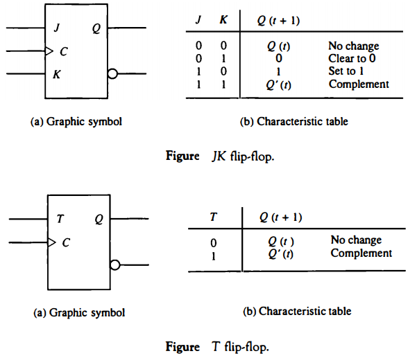
J-K Flip-Flop and T Flip-Flop
A JK flip-flop is a refinement of the SR flip-flop in that the indeterminate condition of the SR type is defined in the JK type.
Inputs J and K behave like inputs S and R to set and clear the flip-flop, respectively.
When inputs J and K are both equal to 1, a clock transition switches the outputs of the flip-flop to their complement state.
The graphic symbol and characteristic table of the JK flip-flop are shown in Fig. below.
The J input is equivalent to the S (set) input of the SR flip-flop, and the K input is equivalent to the R (clear) input.
Instead of the indeterminate condition, the JK flip-flop has a complement condition Q(t + 1) = Q'(t) when both J and K are equal to 1.
T Flip-Flop is obtained from a JK type when inputs J and K are connected to provide a single input designated by T.
The T flip-flop therefore has only two conditions. When T = 0 (J = K = 0) a clock transition does not change the state of the flip-flop.
When T = 1 (J = K = 1) a clock transition complements the state of the flip-flop. These conditions can be expressed by a characteristic equation: Q(t + 1) = Q(t) ⊕ T
Edge Triggered Flip Flops
The most common type of flip-flop used to synchronize the state change during a clock pulse transition is the edge-triggered flip-flop.
In this type of flip-flop, output transitions occur at a specific level of the clock pulse.
When the pulse input level exceeds this threshold level, the inputs are locked out so that the flip-flop is unresponsive to further changes in inputs until the clock pulse returns to 0 and another pulse occurs.
Some edge-triggered flip-flops cause a transition on the rising edge of the clock signal (positive-edge transition), and others cause a transition on the falling edge (negative-edge transition).
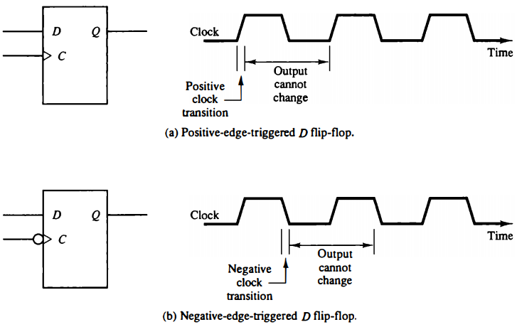
Figure below shows the clock pulse signal in a positive-edge-triggered D flip-flop.
The value in the D input is transferred to the Q output when the clock makes a positive transition.
The output cannot change when the clock is in the 1 level, in the 0 level, or in a transition from the 1 level to the 0 level.
The effective positive clock transition includes a minimum time called the setup time in which the D input must remain at a constant value before the transition, and a definite time called the hold time in which the D input must not change after the positive transition. The effective positive transition is usually a very small fraction of the total period of the clock pulse.
Figure below shows the corresponding graphic symbol and timing diagram for a negative-edge-triggered D flip-flop.
The graphic symbol includes a negation small circle in front of the dynamic indicator at the C input. This denotes a negative-edge-triggered behavior.
In this case the flip-flop responds to a transition from the 1 level to the 0 level of the clock signal.
Another type of flip-flop used in some systems is the master-slave flipflop. This type of circuit consists of two flip-flops. The first is the master, which responds to the positive level of the clock, and the second is the slave, which responds to the negative level of the clock.
The result is that the output changes during the 1-to-0 transition of the clock signal.
The trend is away from the use of master-slave flip-flops and toward edge-triggered flip-flops.
Flip-flops available in integrated circuit packages will sometimes provide special input terminals for setting or clearing the flip-flop asynchronously. These inputs are usually called "preset" and "clear."
They affect the flip-flop on a negative level of the input signal without the need of a clock pulse. These inputs are useful for bringing the flip-flops to an initial state prior to its clocked operation.
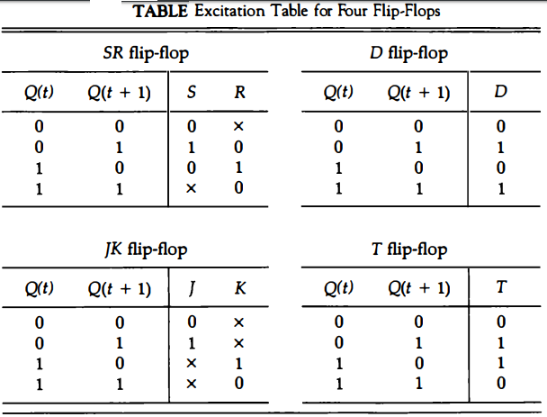
Excitation Tables
The characteristic tables of flip-flops specify the next state when the inputs and the present state are known.
During the design of sequential circuits we usually know the required transition from present state to next state and wish to find the flip-flop input conditions that will cause the required transition.
For this reason we need a table that lists the required input combinations for a given change of state. Such a table is called a flip-flop excitation table.
Tables below lists the excitation tables for the four types of flip-flops. Each table consists of two columns, Q(t) and Q(t + 1), and a column for each input to show how the required transition is achieved.
There are four possible transitions from present state Q(t) to next state Q(t + 1). The required input conditions for each of these transitions are derived from the information available in the characteristic tables.
The symbol x in the tables represents a don't-care condition; that is, it does not matter whether the input to the flip-flop is 0 or 1.
The reason for the don't-care conditions in the excitation tables is that there are two ways of achieving the required transition.
For example, in a JK flip-flop, a transition from present state of 0 to a next state of 0 can be achieved by having inputs J and K equal to 0 (to obtain no change) or by letting J = 0 and K = 1 to clear the flip-flop (although it is already cleared).
In both cases J must be 0, but K is 0 in the first case and 1 in the second. Since the required transition will occur in either case, we mark the K input with a don't-care x and let the designer choose either 0 or 1 for the K input, whichever is more convenient.