Sequential Circuits
A sequential circuit is an interconnection of flip-flops and gates.
The gates by themselves constitute a combinational circuit, but when included with the flip-flops, the overall circuit is classified as a sequential circuit.
The block diagram of a clocked sequential circuit is shown in Fig. below.
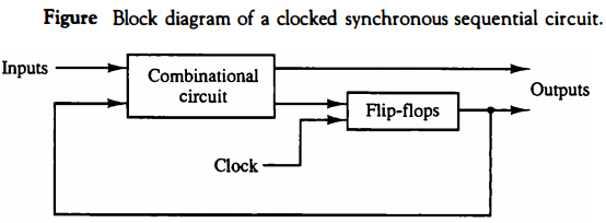
It consists of a combinational circuit and a number of clocked flip-flops. In general, any number or type of flip-flops may be included.
As shown in the diagram, the combinational circuit block receives binary signals from external inputs and from the outputs of flip-flops.
The outputs of the combinational circuit go to external outputs and to inputs of flip-flops. The gates in the combinational circuit determine the binary value to be stored in the flip-flops after each clock transition.
The outputs of flip-flops, in turn, are applied to the combinational circuit inputs and determine the circuit's behavior.
This process demonstrates that the external outputs of a sequential circuit are functions of both external inputs and the present state of the flip-flops.
Moreover, the next state of flip-flops is also a function of their present state and external inputs.
Thus a sequential circuit is specified by a time sequence of external inputs, external outputs, and internal flip-flop binary states.
Flip-Flop Input Equations
An example of a sequential circuit is shown in Fig. below.
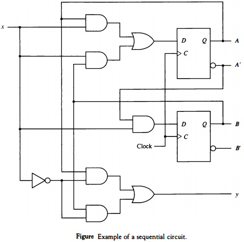
It has one input variable x, one output variable y, and two clocked D flip-flops. The AND gates, OR gates, and inverter form the combinational logic part of the circuit.
The interconnections among the gates in the combinational circuit can be specified by a set of Boolean expressions.
The part of the combinational circuit that generates the inputs to flip-flops are described by a set of Boolean expressions called flip-flop input equations.
We adopt the convention of using the flip-flop input symbol to denote the input equation variable name and a subscript to designate the symbol chosen for the output of the flip-flop. Thus, in Fig. above we have two input equations, designated DA and DB.
The first letter in each symbol denotes the D input of a D flip-flop. The subscript letter is the symbol name of the flip-flop.
The input equations are Boolean functions for flip-flop input variables and can be derived by inspection of the circuit. Since the output of the OR gate is connected to the D input of flip-flop A, we write the first input equation as : DA = A x + B x
where A and B are the outputs of the two flip-flops and x is the external input. The second input equation is derived from the single AND gate whose output is connected to the D input of flip-flop B: DB = A'x
The sequential circuit also has an external output, which is a function of the input variable and the state of the flip-flops. This output can be specified algebraically by the expression : y = Ax' + Bx'
From this example we note that a flip-flop input equation is a Boolean expression for a combinational circuit.
The subscripted variable is a binary variable name for the output of a combinational circuit. This output is always connected to a flip-flop input.
State Table
The behavior of a sequential circuit is determined from the inputs, the outputs, and the state of its flip-flops. Both the outputs and the next state are a function of the inputs and the present state.
A sequential circuit is specified by a state table that relates outputs and next states as a function of inputs and present states. In clocked sequential circuits, the transition from present state to next state is activated by the presence of a clock signal.
The state table for the circuit of Fig. below is shown in Table below.
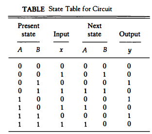
The table consists of four sections, labeled present state, input, next state, and output. The present-state section shows the states of flip-flops A and B at any given time t.
The input section gives a value of x for each possible present state. The next-state section shows the states of the flip-flops one clock period later at time t + 1. The output section gives the value of y for each present state and input condition.
The derivation of a state table consists of first listing all possible binary combinations of present state and inputs. In this case we have eight binary combinations from 000 to 111.
The next-state values are then determined from the logic diagram or from the input equations. The input equation for flip-flop A is DA = Ax + Bx
The next-state value of a each flip-flop is equal to its D input value in the present state. The transition from present state to next state occurs after application of a clock signal.
Therefore, the next state of A is equal to 1 when the present state and input values satisfy the conditions Ax = 1 or Bx = 1, which makes DA equal 1.
This is shown in the state table with three 1's under the column for next state of A. Similarly, the input equation for flip-flop B is DB = A'x
The next state of B in the state table is equal to 1 when the present state of A is 0 and input x is equal to 1. The output column is derived from the output equation
The state table of any sequential circuit is obtained by the procedure used in this example. In general, a sequential circuit with m flip-flops, n input variables, and p output variables will contain m columns for present state, n columns for inputs, m columns for next state, and p columns for outputs.
The present state and input columns are combined and under them we list the 2m + n binary combinations from 0 through 2m + n - 1.
The next-state and output columns are functions of the present state and input values and are derived directly from the circuit or the Boolean equations that describe the circuit.
State Diagram
The information available in a state table can be represented graphically in a state diagram.
In this type of diagram, a state is represented by a circle, and the transition between states is indicated by directed lines connecting the circles.
The state diagram of the sequential circuit is shown in Fig. below.
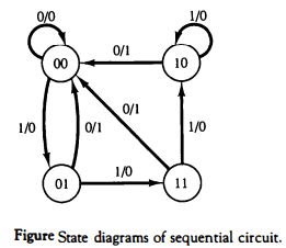
The state diagram provides the same information as the state table.
The binary number inside each circle identifies the state of the flip-flops.
The directed lines are labeled with two binary numbers separated by a slash. The input value during the present state is labeled first and the number after the slash gives the output during the present state.
For example, the directed line from state 00 to 01 is labeled 1/0, meaning that when the sequential circuit is in the present state 00 and the input is 1, the output is 0.
After a clock transition, the circuit goes to the next state 01 . The same clock transition may change the input value.
If the input changes to 0, the output becomes 1, but if the input remains at 1, the output stays at 0. This information is obtained from the state diagram along the two directed lines emanating from the circle representing state 01.
A directed line connecting a circle with itself indicates that no change of state occurs.
There is no difference between a state table and a state diagram except in the manner of representation. The state table is easier to derive from a given logic diagram and the state diagram follows directly from the state table.
The state diagram gives a pictorial view of state transitions and is the form suitable for human interpretation of the circuit operation.
For example, the state diagram of Fig. above clearly shows that starting from state 00, the output is 0 as long as the input stays at 1.
The first 0 input after a string of 1's gives an output of 1 and transfers the circuit back to the initial state 00.
Design Example
The design procedure consists of first translating the circuit specifications into a state diagram. The state diagram is then converted into a state table. From the state table we obtain the information for obtaining the logic circuit diagram.
We wish to design a clocked sequential circuit that goes through a sequence of repeated binary states 00, 01, 10, and 11 when an external input x is equal to 1. The state of the circuit remains unchanged when x = 0.
This type of circuit is called a 2-bit binary counter because the state sequence is identical to the count sequence of two binary digits.
Input x is the control variable that specifies when the count should proceed.
The binary counter needs two flip-flops to represent the two bits. The state diagram for the sequential circuit is shown in Fig. below.
The diagram is drawn to show that the states of the circuit follow the binary count as long as
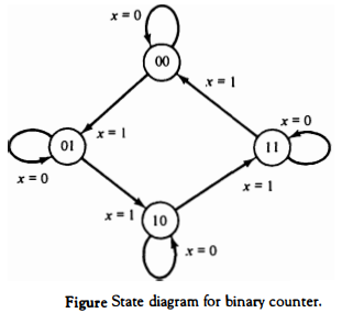
x = 1. The state following 11 is 00, which causes the count to be repeated. If x = 0, the state of the circuit remains unchanged.
This sequential circuit has no external outputs, and therefore only the input value is labeled in the diagram. The state of the flip-flops is considered as the outputs of the counter.
We have already assigned the symbol x to the input variable. We now assign the symbols A and B to the two flip-flop outputs.
The next state of A and B, as a function of the present state and input x, can be transferred from the state diagram into a state table. The first five columns of Table below constitute the state table.
The entries for this table are obtained directly from the state diagram. The excitation table of a sequential circuit is an extension of the state table.
This extension consists of a list of flip-flop input excitations that will cause the
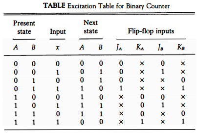
required state transitions.The flip-flop input conditions are a function of the type of flip-flop used. If we employ J-K flip-flops, we need columns for the J and K inputs of each flip-flop. We denote the inputs of flip-flop A by JA and KA, and those of flip-flop B by JB and KB.
The excitation table for the J-K flip-flop specified in Table earlier is now used to derive the excitation table of the sequential circuit.
For example, in the first row of Table above, we have a transition for flip-flop A from 0 in the present state to 0 in the next state.
In excitation table for the J-K flip-flop we find that a transition of states from Q(t) = 0 to Q(t + 1) = 0 in a J-K flip-flop requires that input J = 0 and input K = x. So 0 and x are copied in the first row under JA and KA, respectively.
Since the first row also shows a transition for flip-flop B from 0 in the present state to 0 in the next state, 0 and x are copied in the first row under JB and KB.
The second row of Table above shows a transition for flip-flop B from 0 in the present state to 1 in the next state.
From excitation table for the J-K flip-flop we find that a transition from Q(t) = 0 to Q(t + 1) = 1 requires that input J = 1 and input K = x. So 1 and x are copied in the second row under JB and KB, respectively.
This process is continued for each row of the table and for each flip-flop, with the input conditions as specified in excitation table for the J-K flip-flop being copied into the proper row of the particular flip-flop being considered.
Let us now consider the information available in an excitation table such as Table 1-5. We know that a sequential circuit consists of a number of flip-flops and a combinational circuit.
From the block diagram of Fig. Block diagram of a clocked synchronous sequential circuit, we note that the outputs of the combinational circuit must go to the four flip-flop inputs JA and KA, JB and KB.
The inputs to the combinational circuit are the external input x and the present-state values of flip-flops A and B.
Moreover, the Boolean functions that specify a combinational circuit are derived from a truth table that shows the input-output relationship of the circuit.
The entries that list the combinational circuit inputs are specified under the "present state" and "input" columns in the excitation table.
The combinational circuit outputs are specified under the "flip-flop inputs" columns. Thus an excitation table transforms a state diagram to a truth table needed for the design of the combinational circuit part of the sequential circuit.
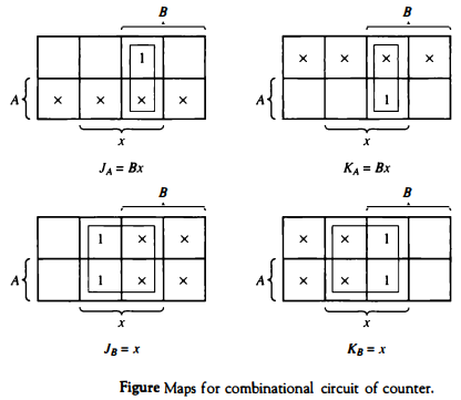
The simplified Boolean functions for the combinational circuit can now be derived. The inputs are the variables A, B, and x.
The outputs are the variables JA and KA, JB and KB.
The information from the excitation table is transferred into the maps of Fig. Maps for combinational circuit of counter. , where the four simplified flip-flop input equations are derived:
JA = Bx
JB = x
KA = Bx
KB = x
The logic diagram is drawn in Fig. Logic diagram of a 2-bit binary counter. and consists of two J-K flip-flops and an AND gate.
Note that inputs J and K determine the next state of the counter when a clock signal occurs. If both J and K are equal to 0, a clock signal will
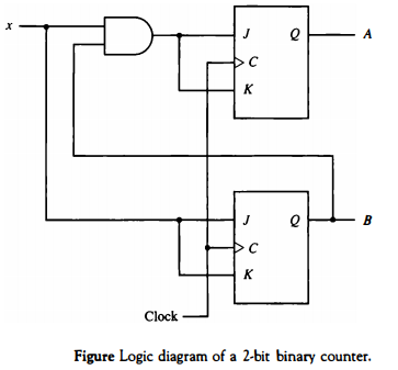
have no effect; that is, the state of the flip-flops will not change. Thus when x = 0, all four inputs of the flip-flops are equal to 0 and the state of the flip-flops remains unchanged even though clock pulses are applied continuously.
Design Procedure
The design of sequential circuits follows the outline described in the preceding example.
The behavior of the circuit is first formulated in a state diagram.
The number of flip-flops needed for the circuit is determined from the number of bits listed within the circles of the state diagram. The number of inputs for the circuit is specified along the directed lines between the circles.
We then assign letters to designate all flip-flops and input and output variables and proceed to obtain the state table. For m flip-flops and n inputs, the state table will consist of m columns for the present state, n columns for the inputs, and m columns for the next state.
The number of rows in the table will be up to 2m + n, one row for each binary combination of present state and inputs.
For each row we list the next state as specified by the state diagram. Next, the flip-flop type to be used in the circuit is chosen. The state table is then extended into an excitation table by including columns for each input of each flip-flop.
The excitation table for the type of flip-flop in use can be found in Table Excitation Table for Four Flip-Flops .
From the information available in this table and by inspecting present state-to-next state transitions in the state table, we obtain the information for the flop-flop input conditions in the excitation table.
The truth table for the combinational circuit part of the sequential circuit is available in the excitation table. The present-state and input columns constitute the inputs in the truth table.
The flip-flop input conditions constitute the outputs in the truth table. By means of map simplification we obtain a set of flip-flop input equations for the combinational circuit.
Each flip-flop input equation specifies a logic diagram whose output must be connected to one of the flip-flop inputs. The combinational circuit so obtained, together with the flip-flops, constitutes the sequential circuit.
The outputs of flip-flops are often considered to be part of the outputs of the sequential circuit. However, the combinational circuit may also contain external outputs.
In such a case the Boolean functions for the external outputs are derived from the state table by combinational circuit design techniques. A set of flip-flop input equations specifies a sequential circuit in algebraic form.
The procedure for obtaining the logic diagram from a set of flip-flop input equations is a straightforward process.
First draw the flip-flops and label all their inputs and outputs. Then draw the combinational circuit from the Boolean expressions given by the flip-flop input equations.
Finally, connect outputs of flip-flops to inputs in the combinational circuit and outputs of the combinational circuit to flip-flop inputs.