Integrated Circuits
Digital circuits are constructed with integrated circuits. An integrated circuit (abbreviated IC) is a small silicon semiconductor crystal called a chip containing the electronic components for the digital gates.
The various gates are interconnected inside the chip to form the required circuit.
The chip is mounted in a ceramic or plastic container, and connections are welded by thin gold wires to external pins to form the integrated circuit.
The number of pins may range from 14 in a small IC package to 100 or more in a larger package. Each IC has a numeric designation printed on the surface of the package for identification.
Small-scale integration (SSI) devices contain several independent gates in a single package. The inputs and outputs of the gates are connected directly to the pins in the package. The number of gates is usually less than 10 and is limited by the number of pins available in the IC.
Medium-scale integration (MSI) devices have a complexity of approximately 10 to 200 gates in a single package. They usually perform specific elementary digital functions such as decoders, adders, and registers.
Large-scale integration (LSI) devices contain between 200 and a few thousand gates in a single package. They include digital systems, such as processors, memory chips, and programmable modules.
Very-large-scale integration (VLSI) devices contain thousands of gates within a single package. Examples are large memory arrays and complex microcomputer chips.
Many different logic families of integrated circuits have been introduced commercially. The following are the most popular.
Transistor-transistor logic
Emitter-coupled logic
Metal-oxide semiconductor
Complementary metal-oxide semiconductor
TTL is a widespread logic family that has been in operation for many years and is considered as standard. ECL has an advantage in systems requiring high-speed operation. MOS is suitable for circuits that need high component density, and CMOS is preferable in systems requiring low power consumption.
Decoders
Discrete quantities of information are represented in digital computers with binary codes. A binary code of n bits is capable of representing up to 2n distinct elements of the coded information.
A decoder is a combinational circuit that converts binary information from the n coded inputs to a maximum of 2n unique outputs.
If the n-bit coded information has unused bit combinations, the decoder may have less than 2n outputs.
The decoders presented in this section are called n-to-m-line decoders, where m ≤ 2n. Their purpose is to generate the 2n (or fewer) binary combinations of the n input variables. A decoder has n inputs and m outputs and is also referred to as an n x m decoder.
The logic diagram of a 3-to-8-line decoder is shown in Fig. below The three data inputs, A0, A1 and A2, are decoded into eight outputs, each output
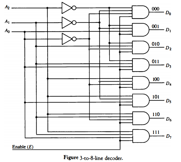
representing one of the combinations of the three binary input variables. The three inverters provide the complement of the inputs, and each of the eight AND gates generates one of the binary combination.
A particular application of this decoder is a binary-to-octal conversion. The input variables represent a binary number and the outputs represent the eight digits of the octal number system.
However, a 3-to-8-line decoder can be used for decoding any 3-bit code to provide eight outputs, one for each combination of the binary code. Commercial decoders include one or more enable inputs to control the operation of the circuit. The decoder of Fig. 2-1 has one enable input, E.
The decoder is enabled when E is equal to 1 and disabled when E is equal to 0. The operation of the decoder can be clarified using the truth table listed in Table 2-1 . When the enable input E is equal to 0, all the outputs are equal to 0 regardless of the values of the other three data inputs.
The three x's in the table designate don't-care conditions. When the enable input is equal to I, the decoder operates in a normal fashion. For each possible input combination, there are seven outputs that are equal to 0 and only one that is equal to I.
The output variable whose value is equal to 1 represents the octal number equivalent of the binary number that is available in the input data lines.
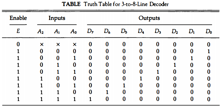
NAND Gate Decoder
Some decoders are constructed with NAND instead of AND gates. Since a NAND gate produces the AND operation with an inverted output, it becomes more economical to generate the decoder outputs in their complement form.
A 2-to-4-line decoder with an enable input constructed with NAND gates is shown in Fig. below. The circuit operates with complemented outputs and a complemented enable input E.
The decoder is enabled when E is equal to 0. As indicated by the truth table, only one output is equal to 0 at any given time; the other three outputs are equal to 1.
The output whose value is equal to 0 represents the equivalent binary number in inputs A1 and A0. The circuit is disabled when E is equal to 1, regardless of the values of the other two inputs.
When the circuit is disabled, none of the outputs are selected and all outputs are equal to 1.
In general, a decoder may operate with complemented or uncomplemented outputs. The enable input may be activated with a 0 or with a 1 signal level.
Some decoders have two or more enable inputs that must satisfy a given logic condition in order to enable the circuit.
Decoder Expansion
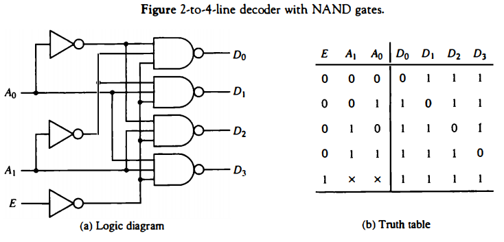
There are occasions when a certain-size decoder is needed but only smaller sizes are available. When this occurs it is possible to combine two or more decoders with enable inputs to form a larger decoder.
Thus if a 6-to-64-line decoder is needed, it is possible to construct it with four 4-to-16-line decoders.
Figure below shows how decoders with enable inputs can be connected to form a larger decoder.
Two 2-to-4-line decoders are combined to achieve a 3-to-8-line decoder. The two least significant bits of the input are connected to both decoders.
The most significant bit is connected to the enable input of one decoder and through an inverter to the enable input of the other decoder.
It is assumed that each decoder is enabled when its E input is equal to 1.
When E is equal to 0, the decoder is disabled and all its outputs are in the O level. When A2 = 0, the upper decoder is enabled and the lower is disabled.
The lower decoder outputs become inactive with all outputs at 0. The outputs of the upper decoder generate outputs D0 through D3, depending on the values of A1 and A0 (while A2 = 0).
When A2 = 1, the lower decoder is enabled and the upper is disabled. The lower decoder output generates the binary equivalent D4 through D7 since these binary numbers have a 1 in the A2 position.
The example demonstrates the usefulness of the enable input in decoders or any other combinational logic component. Enable inputs are a convenient feature for interconnecting two or more circuits for the purpose of expanding the digital component into a similar function but with more inputs and outputs.
Encoders
An encoder is a digital circuit that performs the inverse operation of a decoder.
An encoder has 2n (or less) input lines and n output lines. The output lines generate the binary code corresponding to the input value. An example of an encoder is the octal-to-binary encoder, whose truth table is given in Table below.
It has eight inputs, one for each of the octal digits, and three outputs that generate the corresponding binary number. It is assumed that only one input has a value of 1 at any given time; otherwise, the circuit has no meaning.
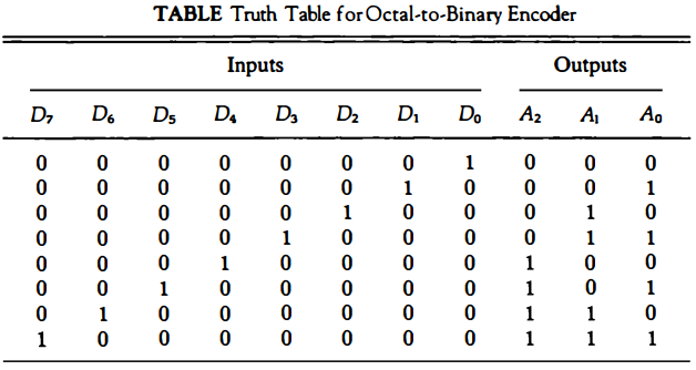
The encoder can be implemented with OR gates whose inputs are determined directly from the truth table. Output A0 = 1 if the input octal digit is 1 or 3 or 5 or 7.
Similar conditions apply for the other two outputs. These conditions can be expressed by the following Boolean functions:
A0 = D1 + D3 + D5 + D7
A1 = D2 + D3 + D6 + D7
A2 = D4 + D5 + D6 + D7
The encoder can be implemented with three OR gates.
Multiplexers
A multiplexer is a combinational circuit that receives binary information from one of 2n input data lines and directs it to a single output line.
The selection of a particular input data line for the output is determined by a set of selection inputs.
A 2n-to-1 multiplexer has 2n input data lines and n input selection lines whose bit combinations determine which input data are selected for the output.
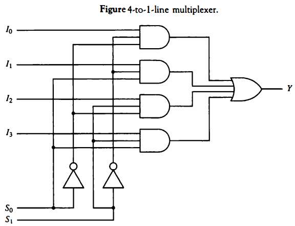
A 4-to-1-line multiplexer is shown in Fig. below. Each of the four data inputs I0 through I3 is applied to one input of an AND gate. The two selection inputs S1 and S0 are decoded to select a particular AND gate. The outputs of the AND gates are applied to a single OR gate to provide the single output.
To demonstrate the circuit operation, consider the case when S1S0 = 10. The AND gate associated with input I2 has two of its inputs equal to 1. The third input of the gate is connected to I2 The other three AND gates have at least one input equal to 0, which makes their outputs equal to 0.
The OR gate output is now equal to the value of I2, thus providing a path from the selected input to the output. The 4-to-1 line multiplexer of Fig. below has six inputs and one output.
A truth table describing the circuit needs 64 rows since six input variables can have 26 binary combinations. This is an excessively long table and will not be shown here.
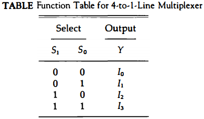
A more convenient way to describe the operation of multiplexers is by means of a function table. The function table for the multiplexer is shown in Table below. The table demonstrates the relationship between the four data inputs and the single output as a function of the selection inputs S1 and S0.
When the selection inputs are equal to 00, output Y is equal to input I0 When the selection inputs are equal to 01, input I1 has a path to output Y, and similarly for the other two combinations.
The multiplexer is also called a data selector, since it selects one of many data inputs and steers the binary information to the output.
The AND gates and inverters in the multiplexer resemble a decoder circuit, and indeed they decode the input selection lines. In general, a 2n-to-1- line multiplexer is constructed from an n-to-2n decoder by adding to it 2n input lines, one from each data input.
The size of the multiplexer is specified by the number 2n of its data inputs and the single output. It is then implied that it also contains n input selection lines.
The multiplexer is often abbreviated as MUX. As in decoders, multiplexers may have an enable input to control the operation of the unit. When the enable input is in the inactive state, the outputs are disabled, and when it is in the active state, the circuit functions as a normal multiplexer.
The enable input is useful for expanding two or more multiplexers to a multiplexer with a larger number of inputs. In some cases two or more multiplexers are enclosed within a single integrated circuit package.
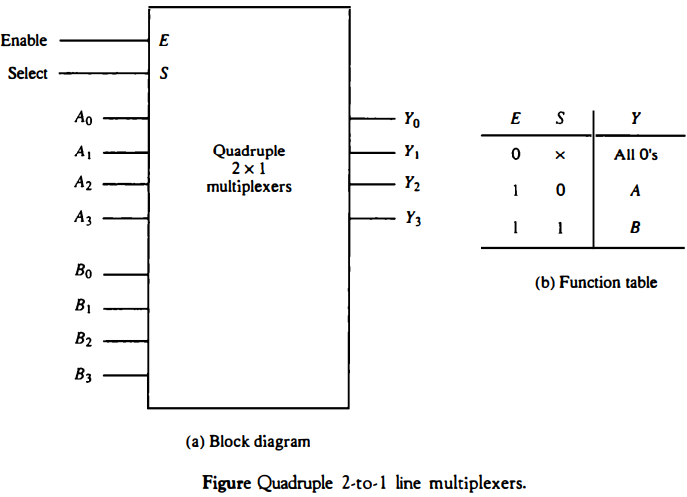
The selection and the enable inputs in multiple-unit construction are usually common to all multiplexers. As an illustration, the block diagram of a quadruple 2-to-1-line multiplexer is shown in Fig. below The circuit has four multiplexers, each capable of selecting one of two input lines. Output Y0 can be selected to come from either input A0 or B0.
Similarly, output Y1 may have the value of A1 or B1 , and so on. One input selection line S selects one of the lines in each of the four multiplexers.
The enable input E must be active for normal operation. Although the circuit contains four multiplexers, we can also think of it as a circuit that selects one of two 4-bit data lines.
As shown in the function table, the unit is enabled when E = 1. Then, if S = 0, the four A inputs have a path to the four outputs. On the other hand, if S = 1, the four B inputs are applied to the outputs. The outputs have all O's when E = 0, regardless of the values of S.
Registers
A register is a group of flip-flops with each flip-flop capable of storing one bit of information.
An n-bit register has a group of n flip-flops and is capable of storing any binary information of n bits. In addition to the flip-flops, a register may have combinational gates that perform certain data-processing tasks.
In its broadest definition, a register consists of a group of flip-flops and gates that effect their transition. The flip-flops hold the binary information and the gates control when and how new information is transferred into the register.
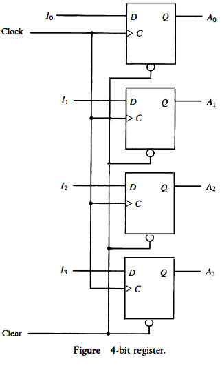
Various types of registers are available commercially. The simplest register is one that consists only of flip-flops, with no external gates. Figure below shows such a register constructed with four D flip-flops.
The common clock input triggers all flip-flops on the rising edge of each pulse, and the binary data available at the four inputs are transferred into the 4-bit register. The four outputs can be sampled at any time to obtain the binary information stored in the register.
The clear input goes to a special terminal in each flip-flop. When this input goes to 0, all flip-flops are reset asynchronously. The clear input is useful for clearing the register to all 0's prior to its clocked operation.
The clear input must be maintained at logic 1 during normal clocked operation. Note that the clock signal enables the D input but that the clear. input is independent of the clock.
The transfer of new information into a register is referred to as loading the register.
If all the bits of the register are loaded simultaneously with a common
clock pulse transition, we say that the loading is done in parallel.A clock transition applied to the C inputs of the register of Fig. above will load all four inputs I0 through I3 in parallel.
In this configuration, the clock must be inhibited from the circuit if the content of the register must be left unchanged.
Shift Registers
A register capable of shifting its binary information in one or both directions is called a shift register.
The logical configuration of a shift register consists of a chain of flip-flops in cascade, with the output of one flip-flop connected to the input of the next flip-flop.
All flip-flops receive common clock pulses that initiate the shift from one stage to the next.
The simplest possible shift register is one that uses only flip-flops, as shown in Fig. below. The output of a given flip-flop is connected to the D input of the flip-flop at its right.
The clock is common to all flip-flops. The serial input determines what goes into the leftmost position during the shift. The serial output is taken from the output of the rightmost flip-flop.
Sometimes it is necessary to control the shift so that it occurs with certain clock pulses but not with others. This can be done by inhibiting the clock from the input of the register if we do not want it to shift. When the shift register of Fig below is used, the shift can be controlled by connecting the clock to the input of an AND gate, and a second input of the AND gate can then control the shift by inhibiting the clock.
However, it is also possible to provide extra circuits to control the shift operation through the D inputs of the flip-flops rather than the clock input.
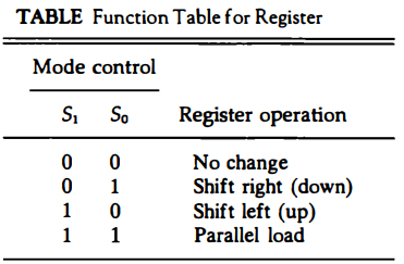
Bidirectional Shift Register with Parallel Load
A register capable of shifting in one direction only is called a unldirectional shift register.
A register that can shift in both directions is called a bidirectional shift register. Some shift registers provide the necessary input and output terminals

for parallel transfer.The most general shift register has all the capabilities listed below. Others may have some of these capabilities, with at least one shift operation.
An input for clock pulses to synchronize all operations.
A shift-right operation and a serial input line associated with the shiftright.
A shift-left operation and a serial input line associated with the shift-left.
A parallel load operation and n input lines associated with the parallel transfer.
n parallel output lines.
A control state that leaves the information in the register unchanged even though clock pulses are applied continuously.
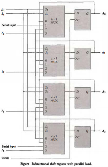
A 4-bit bidirectional shift register with parallel load is shown in Fig. below. Each stage consists of a D flip-flop and a 4 x 1 multiplexer. The two selection inputs S1 and S0 select one of the multiplexer data inputs for the D flip-flop.
The selection lines control the mode of operation of the register according to the function table shown in Table below. When the mode control S1S0 = 00, data input 0 of each multiplexer is selected. This condition forms a path from the output of each flip-flop into the input of the same flip-flop.
The next clock transition transfers into each flip-flop the binary value it held previously, and no change of state occurs.
When S1S0 = 01, the terminal marked 1 in each multiplexer has a path to the D input of the corresponding flip-flop.
This causes a shift-right operation, with the serial input data transferred into flip-flop A0 and the content of each flip-flop Ai-1 transferred into flip-flop Ai for i = 1, 2, 3.
When S1S0 = 10 a shift-left operation results, with the other serial input data going into flip-flop A, and the content of flip-flop Ai+1 transferred into flip-flop Ai for i = 0, 1, 2. When S1S0 = 11, the binary information from each input I0 through I3 is transferred into the corresponding flip-flop, resulting in a parallel load operation.
Note that the way the diagram is drawn, the shift-right operation shifts the contents of the register in the down direction while the shift left operation causes the contents of the register to shift in the upward direction.
Shift registers are often used to interlace digital systems situated remotely from each other. For example, suppose that it is necessary to transmit an n-bit quantity between two points. If the distance between the source and the destination is too far, it will be expensive to use n lines to transmit the n bits In parallel.
It may be more economical to use a single line and transmit the information serially one bit at a time.
The transmitter loads the n-bit data in parallel into a shift register and then transmits the data from the serial output line. The receiver accepts the data serially into a shift register through its serial input line.
When the entire n bits are accumulated they can be taken from the outputs of the register in parallel. Thus the transmitter performs a parallel-to-serial conversion of data and the receiver converts the incoming serial data back to parallel data transfer.