Binary Counters
A register that goes through a predetermined sequence of states upon the application of input pulses is called a counter.
The input pulses may be clock pulses or may originate from an external source. They may occur at uniform intervals of time or at random.
Counters are found in almost all equipment containing digital logic. They are used for counting the number of occurrences of an event and are useful for generating timing signals to control the sequence of operations in digital computers.
Of the various sequences a counter may follow, the straight binary sequence is the simplest and most straightforward. A counter that follows the binary number sequence is called a binary counter. An n-bit binary counter is a register of n flip-flops and associated gates that follows a sequence of states according to the binary count of n bits, from 0 to 2n - 1.
The design of binary counters can be carried out by the procedure outlined in Sec. 1-7 for sequential circuits.
A simpler alternative design procedure may be carried out from a direct inspection of the sequence of states that the register must undergo to achieve a straight binary count.
Going through a sequence of binary numbers such as 0000, 0001, 0010, 0011, and so on, we note that the lower-order bit is complemented after every count and every other bit is complemented from one count to the next if and only if all its lower-order bits are equal to 1.
For example, the binary count from 0111 (7) to 1000 (8) is obtained by (a) complementing the low-order bit, (b) complementing the second-order bit because the first bit of 0111 is 1, (c) complementing the third-order bit because the first two bits of 0111 are 1' s, and (d) complementing the fourth-order bit because the first three bits of 0111 are ali i's.
A counter circuit will usually employ flip-flops with complementing capabilities. Both T and JK flip-flops have this property. Remember that a JK flip-flop is complemented if both its J and K inputs are 1 and the clock goes through a positive transition. The output of the flip-flop does not change if J = K = 0.
In addition, the counter may be controlled with an enable input that turns the counter on or off without removing the clock signal from the flipflops.
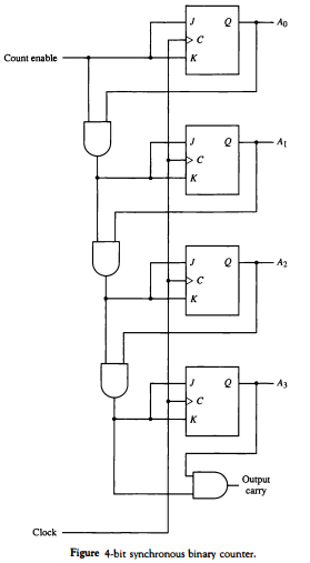
Synchronous binary counters have a regular pattern, as can be seen from the 4-bit binary counter shown in Fig. below. The C inputs of all flip-flops receive the common clock.
If the count enable is 0, all J and K inputs are maintained
 at 0 and the output of the counter does not change.
The first stage A0 is complemented when the counter is enabled and the clock goes through a positive transition. Each of the other three flip-flops are complemented when all previous least significant flip-flops are equal to 1 and the count is enabled.
The chain of AND gates generate the required logic for the J and K inputs. The output carry can be used to extend the counter to more stages, with each stage having an additional flip-flop and an AND gate.
Binary Counter with Parallel Load
Counters employed in digital systems quite often require a parallel load capability for transferring an initial binary number prior to the count operation.
Figure below shows the logic diagram of a binary counter that has a parallel load capability and can also be cleared to 0 synchronous with the clock.
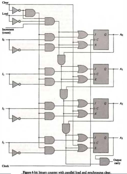
When equal to 1, the clear input sets all the K inputs to 1, thus clearing all flip-flops with the next clock transition.
The input load control when equal to 1, disables the count operation and causes a transfer of data from the four parallel inputs into the four flip-flops (provided that the clear input is 0).
If the clear and load inputs are both 0 and the increment input is 1, the circuit operates as a binary counter.
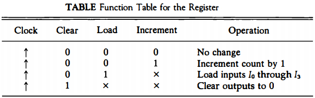
The operation of the circuit is summarized in Table below. With the clear, load, and increment inputs all at 0, the outputs do not change even when pulses are applied to the C terminals.
If the clear and load inputs are maintained at logic 0, the increment input controls the operation of the counter and the outputs change to the next binary count for each positive transition of the clock.
The input data are loaded into the flip-flops when the load control input is equal to 1 provided that the clear is disabled, but the increment input can be 0 or 1. The register is cleared to 0 with the clear control regardless of the values in the load and increment inputs.
Counters with parallel load are very useful in the design of digital computers. In subsequent chapters we refer to them as registers with load and increment operations.
The increment operation adds one to the content of a register. By enabling the count input during one clock period, the content of the register can be incremented by one.
Memory Unit
A memory unit is a collection of storage cells together with associated circuits needed to transfer information in and out of storage.
The memory stores binary information in groups of bits called words. A word in memory is an entity of bits that move in and out of storage as a unit.
A memory word is a group of 1's and 0's and may represent a number, an instruction code, one or more alphanumeric characters, or any other binary-coded information.
A group of byte eight bits is called a byte. Most computer memories use words whose number of bits is a multiple of 8. Thus a 16-bit word contains two bytes, and a 32-bit word is made up of four bytes. The capacity of memories in commercial computers is usually stated as the total number of bytes that can be stored.
The internal structure of a memory unit is specified by the number of words it contains and the number of bits in each word. Special input lines called address lines select one particular word.
Each word in memory is assigned an identification number, called an address, starting from 0 and continuing with 1, 2, 3, up to 2k - 1 where k is the number of address lines. The selection of a specific word inside the memory is done by applying the k-bit binary address to the address lines.
A decoder inside the memory accepts this address and opens the paths needed to select the bits of the specified word. Computer memories may range from 1024 words, requiring an address of 10 bits, to 232 words, requiring 32 address bits.
It is customary to refer to the number of words (or bytes) in a memory with one of the letters K (kilo), M (mega), or G (giga). K is equal to 210, M is equal to 220, and G is equal to 230. Thus 64K = 216, 2M= 221, and 4G = 232.
Two major types of memories are used in computer systems: randomaccess memory (RAM) and read-only memory (ROM).
Random-Access Memory
In random-access memory (RAM) the memory cells can be accessed for information transfer from any desired random location.
That is, the process of locating a word in memory is the same and requires an equal amount of time no matter where the cells are located physically in memory: thus the name "random access."
Communication between a memory and its environment is achieved through data input and output lines, address selection lines, and control lines that specify the direction of transfer.
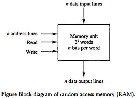
A block diagram of a RAM unit is shown in Fig. below. The n data input lines provide the information to be stored in memory, and the n data output lines supply the information coming out of memory.
The k address lines provide a binary number of k bits that specify a particular word chosen among the 2k available inside the memory. The two control inputs specify the direction of transfer desired.
The two operations that a random-access memory can perform are the write and read operations.
The write signal specifies a transfer-in operation and the read signal specifies a transfer-out operation. On accepting one of these control signals, the internal circuits inside the memory provide the desired function.
The steps that must be taken for the purpose of transferring a new word to be stored into memory are as follows:
Apply the binary address of the desired word into the address lines
Apply the data bits that must be stored in memory into the data input lines.
Activate the write input.
The memory unit will then take the bits presently available in the input data lines and store them in the word specified by the address lines. The steps that must be taken for the purpose of transferring a stored word out of memory are as follows:
1. Apply the binary address of the desired word into the address lines.
2. Activate the read input.
The memory unit will then take the bits from the word that has been selected by the address and apply them into the output data lines. The content of the selected word does not change after reading.
Read-Only Memory
As the name implies, a read-only memory (ROM) is a memory unit that performs the read operation only; it does not have a write capability.
This implies that the binary information stored in a ROM is made permanent during the hardware production of the unit and cannot be altered by writing different words into it.
Whereas a RAM is a general-purpose device whose contents can be altered during the computational process, a ROM is restricted to reading words that are permanently stored within the unit.
The binary information to be stored, specified by the designer, is then embedded in the unit to form the reqttired interconnection pattern.
ROMs come with special internal electronic fuses that can be "programmed" for a specific configuration. Once the pattern is established, it stays within the unit even when power is turned off and on again.
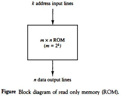
An m x n ROM is an array of binary cells organized into m words of n bits each.
As shown in the block diagram of Fig. above, a ROM has k address input lines to select one of 2k = m words of memory, and n output lines, one for each bit of the word.
An integrated circuit ROM may also have one or more enable inputs for expanding a number of packages into a ROM with larger capacity.
The ROM does not need a read-control line since at any given time, the output lines automatically provide the n bits of the word selected by the address value.
Because the outputs are a function of only the present inputs (the address lines), a ROM is classified as a combinational circuit.
In fact, a ROM is constructed internally with decoders and a set of OR gates.
There is no need for providing storage capabilities as in a RAM, since the values of the bits in the ROM are permanently fixed.
ROMs find a wide range of applications in the design of digital systems. Basically, a ROM generates an input--<>utput relation specified by a truth table.
As such, it can implement any combinational circuit with k inputs and n outputs. When employed in a computer system as a memory unit, the ROM is used for storing fixed programs that are not to be altered and for tables of constants that are not subject to change.
ROM is also employed in the design of control units for digital computers. As such, they are used to store coded information that represents the sequence of internal control variables needed for enabling the various operations in the computer.
A control unit that utilizes a ROM to store binary control information is called a microprogrammed control unit.
Data Types
Binary information in digital computers is stored in memory or processor registers. Registers contain either data or control information.
Control information Is a bit or a group of bits used to specify the sequence of command signals needed for manipulation of the data in other registers.
The data types found in the registers of digital computers may be classified as being one of the following categories: (1) numbers used in arithmetic computations, (2) letters of the alphabet used in data processing. and (3) other discrete symbols used for specific purposes.
All types of data, except binary numbers, are represented in computer registers in binary coded form. This is because registers are made up of flip-flops and flip-flops are two-state devices that can store only 1's and 0's.
The binary number system is the most natural system to use in a digital computer.
But sometimes it is convenient to employ different number systems, especially the decimal number system, since it is used by people to perform arithmetic computations.