Register Transfer Language
A digital system is an interconnection of digital hardware module that accomplish a specific information-processing task.
Digital system design invariably use a modular approach. The modules are constructed from such digital components as registers, decoders, arithmetic elements and control logic.
Digital modules are best defined by the registers they contain and the operations that are performed on the data stored in them.
The operations on data stored in registers are called micro-operations. A microoperation is an elementary operation performed on the information stored in one or more registers.
The result of the operation may replace the previous binary information of a register or may be transferred to another register.
Examples of microoperations introduced are shift, count, clear, and load.
Registers implement micro-operations a counter with parallel load is capable of performing the micro-operations increment and load. A bidirectional shift register is capable of performing the shift right and shift left microoperations.
The internal hardware organization of a digital computer is best defined by specifying:
The set of registers it contains and their function.
The sequence of microoperations performed on the binary information stored in the registers.
The control that initiates the sequence of microoperations.
It is more convenient to adopt a suitable symbology to describe the sequence of transfers between registers and the various arithmetic and logic microoperations associated with the transfers.
The symbolic notation used to describe the microoperation transfers among registers is called a register transfer language. The term "register transfer" implies the availability of hardware logic circuits that can perform a stated microoperation and transfer the result of the operation to the same or another register.
A register transfer language is a system for expressing in symbolic form the microoperation sequences among the registers of a digital module.
It is a convenient tool for describing the internal organization of digital computers in concise and precise manner. It can also be used to facilitate the design process of digital systems.
Register Transfer
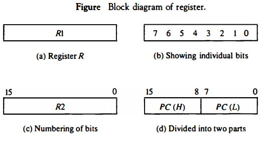
Computer registers are designated by capital letters (sometimes followed by numerals) to denote the function of the register. For example, the register that holds an address for the memory unit is usually called a memory address register and is designated by the name MAR.
Other designations for registers are PC (for program counter), IR (for instruction register, and R1 (for processor register).
The individual flip-flops in an n-bit register are numbered in sequence from 0 through n - 1, starting from 0 in the rightmost position and increasing the numbers toward the left
The most common way to represent a register is by a rectangular box with the name of the register inside.
Information transfer from one register to another is designated in symbolic form by means of a replacement operator. The statement R2 ← R1 denotes a transfer of the content of register R1 into register R2.
It designates a replacement of the content of R2 by the content of R1.
By definition, the content of the source register R1 does not change after the transfer.
A statement that specifies a register transfer implies that circuits are available from the outputs of the source register to the inputs of the destination register and that the destination register has a parallel load capability.
Normally, we want the transfer to occur only under a predetermined control condition. This can be shown by means of an if-then statement.
If (P = 1) then (R2 ← R1) where P is a control signal generated in the control section. It is sometimes convenient to separate the control variables from the register transfer operation by specifying a control function.
A control function is a Boolean variable that is equal to 1 or 0. The control function is included in the statement as follows: P: R2 ← R1
The control condition is terminated with a colon. It symbolizes the requirement that the transfer operation be executed by the hardware only if P = 1.
Every statement written in a register transfer notation implies a hardware construction for implementing the transfer. Figure below shows the block diagram that depicts the transfer from R1 to R2. The n outputs of register R1 are connected to the n inputs of register R2.
The letter n will be used to indicate any number of bits for the register. It will be replaced by an actual number when the length of the register is known. Register R2 has a load input that is activated by the control variable P.
It is assumed that the control variable is synchronized with the same clock as the one applied to the register. As shown
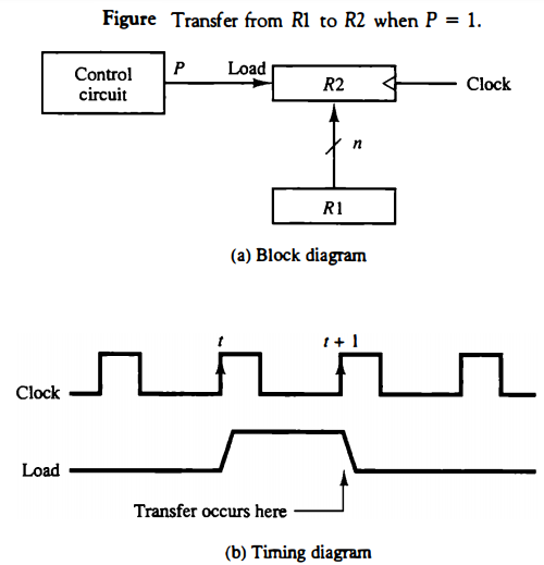
in the timing diagram, P is activated in the control section by the rising edge of a clock pulse at time t. The next positive transition of the clock at time t + 1 finds the load input active and the data inputs of R2 are then loaded into the register in parallel.P may go back to 0 at time t + 1; otherwise, the transfer will occur with every clock pulse transition while P remains active. Note that the clock is not included as a variable in the register transfer statements. It is assumed that all transfers occur during a clock edge transition.
Even though the control condition such as P becomes active just after time t, the actual transfer does not occur until the register is triggered by the next positive transition of the clock at time t + 1.
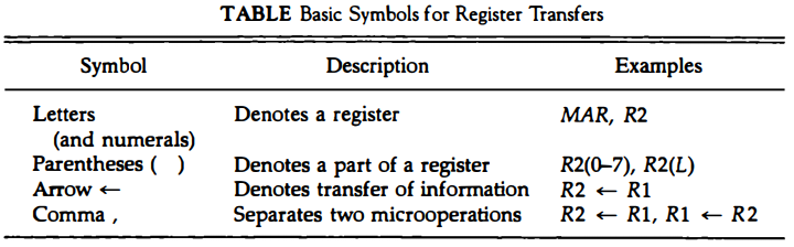
The basic symbols of the register transfer notation are listed in Table above. Registers are denoted by capital letters, and numerals may follow the letters. Parentheses are used to denote a part of a register by specifying the range of bits or by giving a symbol name to a portion of a register.
The arrow denotes a transfer of information and the direction of transfer. A comma is used to separate two or more operations that are executed at the same time.
The statement T: R2 ← R1, R1 ← R2 denotes an operation that exchanges the contents of two registers during one common clock pulse provided that T = 1.
This simultaneous operation is possible with registers that have edge-triggered flip-flops.
Bus and Memory Transfers
A typical digital computer has many registers, and paths must be provided to transfer information from one register to another.
The number of wires will be excessive if separate lines are used between each register and all other registers in the system.
A more efficient scheme for transferring information between registers in a multiple-register configuration is a common bus system.
A bus structure consists of a set of common lines, one for each bit of a register, through which binary information is transferred one at a time. Control signals determine which register is selected by the bus during each particular register transfer.
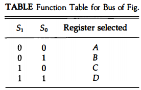
One way of constructing a common bus system is with multiplexers. The multiplexers select the source register whose binary information is then placed on the bus. The construction of a bus system for four registers is shown in Fig. below. Each register has four bits, numbered 0 through 3.
The bus consists of four 4 x 1 multiplexers each having four data inputs, 0 through 3, and two selection inputs, S1 and S0. In order not to complicate the diagram with 16 lines crossing each other, we use labels to show the connections from the outputs of the registers to the inputs of the multiplexers.
For example, output 1 of register A is connected to input 0 of MUX 1 because this input is labeled A1. The diagram shows that the bits in the same significant position in each register are connected to the data inputs of one multiplexer to form one line of the bus.
Thus MUX 0 multiplexes the four 0 bits of the registers, MUX 1 multiplexes the four 1 bits of the registers, and similarly for the other two bits.
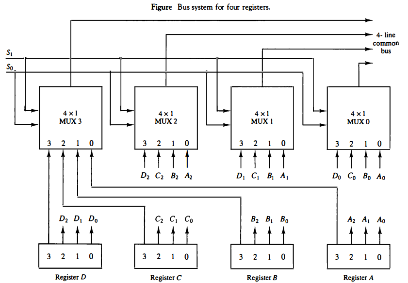
The two selection lines S1 and S0 are connected to the selection inputs of all four multiplexers.
The selection lines choose the four bits of one register and transfer them into the four-line common bus. When S1S0 = 00, the 0 data inputs of all four multiplexers are selected and applied to the outputs that form the bus.
This causes the bus lines to receive the content of register A since the outputs of this register are connected to the 0 data inputs of the multiplexers.
Similarly, register B is selected if S1S0 = 01, and so on. Table below shows the register that is selected by the bus for each of the four possible binary value of the selection lines.
In general, a bus system will multiplex k registers of n bits each to produce an n-line common bus. The number of multiplexers needed to construct the bus is equal to n, the number of bits in each register. The size of each multiplexer must be k x 1 since it multiplexes k data lines.
For example, a common bus for eight registers of 16 bits each requires 16 multiplexers, one for each line in the bus. Each multiplexer must have eight data input lines and three selection lines to multiplex one significant bit in the eight registers.
The transfer of information from a bus into one of many destination registers can be accomplished by connecting the bus lines to the inputs of all destination registers and activating the load control of the particular destination register selected.
The symbolic statement for a bus transfer may mention the bus or its presence may be implied in the statement. When the bus is includes in the statement, the register transfer is symbolized as follows: BUS ← C, R1 ← BUS
The content of register C is placed on the bus, and the content of the bus is loaded into register R 1 by activating its load control input. If the bus is known to exist in the system, it may be convenient just to show the direct transfer. R1 ← C
From this statement the designer knows which control signals must be activated to produce the transfer through the bus.
Three-State Bus Buffers
A bus system can be constructed with three-state gates instead of multiplexers. A three-state gate is a digital circuit that exhibits three states. Two of the states are signals equivalent to logic 1 and 0 as in a conventional gate.
The third state is a high-impedance state. The high-impedance state behaves like an open circuit, which means that the output is disconnected and does not have a logic significance.
Three-state gates may perform any conventional logic, such as AND or NAND. However, the one most commonly used in the design of a bus system is the buffer gate.
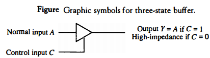
The graphic symbol of a three-state buffer gate is shown in Fig. below. It is distinguished from a normal buffer by having both a normal input and a control input. The control input determines the output state.
When the control input is equal to 1, the output is enabled and the gate behaves like any conventional buffer, with the output equal to the normal input.
When the control input is 0, the output is disabled and the gate goes to a high-impedance state, regardless of the value in the normal input.
The high-impedance state of a three-state gate provides a special feature not available in other gates. Because of this feature, a large number of three-state gate outputs can be connected with wires to form a common bus line without endangering loading effects.
The construction of a bus system with three-state buffers is demonstrated in Fig. below. The outputs of four buffers are connected together to form a single bus line.
(It must be realized that this type of connection cannot be done with gates that do not have three-state outputs.) The control inputs to the buffers determine which of the four normal inputs will communicate with the bus line .
No more than one buffer may be in the active state at any given time. The connected buffers must be controlled so that only one three-state buffer has access to the bus line while all other buffers are maintained in a high impedance state.
One way to ensure that no more than one control input is active at any given time is to use a decoder, as shown in the diagram. When the enable input of the decoder is 0, all of its four outputs are 0, and the bus line is in a high-impedance state because all four buffers are disabled.
When the enable input is active, one of the three-state buffers will be active, depending on the binary value in the select inputs of the decoder. Careful investigation will reveal that Fig. below is another way of constructing a 4 x 1 multiplexer since the circuit can replace the multiplexer in Fig. Bus system for four registers.
To construct a common bus for four registers of n bits each using three
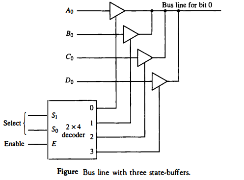
state buffers, we need n circuits with four buffers in each as shown in Fig. above. Each group of four buffers receives one significant bit from the four registers.
Each common output produces one of the lines for the common bus for a total of n lines. Only one decoder is necessary to select between the four registers.
Memory Transfer
The transfer of information from a memory word to the outside environment is called a read operation. The transfer of new information to be stored into the memory is called a write operation.
A memory word will be symbolized by the letter M. The particular memory word among the many available is selected by the memory address during the transfer.
It is necessary to specify the address of M when writing memory transfer operations. This will be done by enclosing the address in square brackets following the letter M.
Consider a memory unit that receives the address from a register, called the address register, symbolized by AR .
The data are transferred to another register, called the data register, symbolized by DR . The read operation can be stated as follows: Read: DR ← M[AR]
This causes a transfer of information into DR from the memory word M selected by the address in AR .
The write operation transfers the content of a data register to a memory word M selected by the address. Assume that the input data are in register R1 R3 ← R1 + R2 + 1. R2 is the symbol for the 1's complement of R2.
Adding 1 to the 1's complement produces the 2' s complement. Adding the contents of R1 to the 2's complement of R2 is equivalent to R1 - R2.
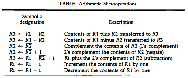
The increment and decrement microoperations are symbolized by plusone and minus-one operations, respectively. These microoperations are implemented with a combinational circuit or with a binary up-down counter.
The arithmetic operations of multiply and divide are not listed in Table above. These two operations are valid arithmetic operations but are not included in the basic set of microoperations.
The only place where these operations can be considered as microoperations is in a digital system, where they are implemented by means of a combinational circuit.
In such a case, the signals that perform these operations propagate through gates, and the result of the operation can be transferred into a destination register by a clock pulse as soon as the output signal propagates through the combinational circuit.
In most computers, the multiplication operation is implemented with a sequence of add and shift microoperations.
Division is implemented with a sequence of subtract and shift microoperations.
To specify the hardware in such a case requires a list of statements that use the basic microoperations of add, subtract, and shift
Binary Adder
To implement the add microoperation with hardware, we need the registers that hold the data and the digital component that performs the arithmetic addition.
The digital circuit that forms the arithmetic sum of two bits and a previous carry is called a full-adder.
The digital circuit that generates the arithmetic sum of two binary numbers of any length is called a binary adder.
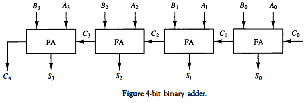
The binary adder is constructed with full-adder circuits connected in cascade, with the output carry from one full-adder connected to the input carry of the next full-adder. Figure below shows the interconnections of four full-adders (FA) to provide a 4-bit binary adder.
The augend bits of A and the addend bits of B are designated by subscript numbers from right to left, with subscript 0 denoting the low-order bit. The carries are connected in a chain through the full-adders.
The input carry to the binary adder is C0 and the output carry is C4. The S outputs of the full-adders generate the required sum bits.
An n-bit binary adder requires n full-adders. The output carry from each full-adder is connected to the input carry of the next-high-order full-adder.
The n data bits for the A inputs come from one register (such as R1), and the n data bits for the B inputs come from another register (such as R2).
The sum can be transferred to a third register or to one of the source registers (R1 or R2), replacing its previous content.
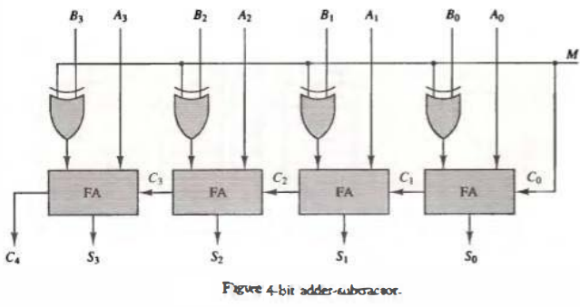
Binary Adder-Subtractor
The subtraction of binary numbers can be done most conveniently by means of complements.
Remember that the subtraction A - B can be done by taking the 2's complement of B and adding it to A.
The 2's complement can be obtained by taking the 1' s complement and adding one to the least significant pair of bits.
The 1's complement can be implemented with inverters and a one can be added to the sum through the input carry.
The addition and subtraction operations can be combined into one common circuit by including an exclusive-OR gate with each full-adder. A 4-bit adder-subtractor circuit is shown in Fig. below.
The mode input M controls the operation. When M = 0 the circuit is an adder and when M = 1 the circuit becomes a subtractor. Each exclusive-OR gate receives input M and one of the inputs of B. When M = 0, we have B ⊕ 0 = B.
The full-adders receive the value of B, the input carry is O, and the circuit performs A plus B. When M = 1, we have B ⊕ 1 = B' and C0 = 1.
The B inputs are all complemented and a 1 is added through the input carry.
The circuit performs the operation A plus the 2's complement of B. For unsigned numbers, this gives A - B if A ≥ B or the 2's complement of (B - A) if A < B. For signed numbers, the result is A - B provided that there Is no overflow.
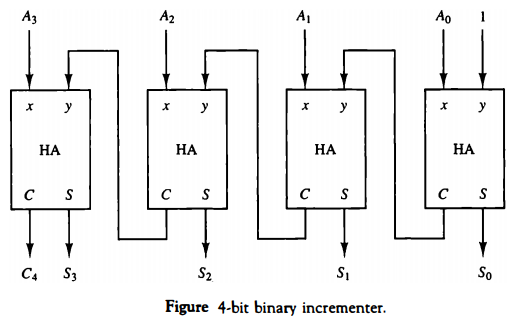
Binary Incrementer
The increment microoperation adds one to a number in a register.
For example, if a 4-bit register has a binary value 0110, it will go to 0111 after it is incremented.
This microoperation is easily implemented with a binary counter. Every time the count enable is active, the clock pulse transition increments the content of the register by one.
There may be occasions when the increment microoperation must be done with a combinational circuit independent of a particular register. This can be accomplished by means of half-adders connected in cascade.
The diagram of a 4-bit combinational drcuit incrementer is shown in Fig. below. One of the inputs to the least significant half-adder (HA) is connected to logic-1 and the other input is connected to the least significant bit of the number to be incremented.
The output carry from one half-adder is connected to one of the inputs of the next-higher-order half-adder. The circuit receives the four bits from A0 through A3. adds one to it, and generates the incremented output in S0 through S3.
The output carry C4 will be 1 only after incrementing binary 1111. This also causes outputs S0 through S3 to go to 0. The circuit of Fig. below can be extended to an n-bit binary incrementer by extending the diagram to include n half-adders.
The least significant bit must have one input connected to logic-1. The other inputs receive the number to be incremented or the carry from the previous stage.
Arithmetic Circuit
The arithmetic microoperations listed in Table below can be implemented in one composite arithmetic circuit.
The basic component of an arithmetic circuit is the parallel adder. By controlling the data inputs to the adder, it is possible to obtain different types of arithmetic operations.
-
The diagram of a 4-bit arithmetic circuit is shown in Fig. below. It has four full-adder circuits that constitute the 4-bit adder and four multiplexers for choosing different operations.
There are two 4-bit inputs A and B and a 4-bit output D. The four inputs from A go directly to the X inputs of the binary adder.
Each of the four inputs from B are connected to the data inputs of the multiplexers. The multiplexers data inputs also receive the complement of B. The other two data inputs are connected to logic-0 and logic-1. Logic-0 is a fixed voltage value (0 volts for TTL integrated circuits) and the logic-1 signal can be generated through an inverter whose input is 0.
The four multiplexers are controlled by two selection inputs, S1 and S0. The input carry Cin goes to the carry input of the FA in the least significant position. The other carries are connected from one stage to the next.
The output of the binary adder is calculated from the following arithmetic sum: D =A + Y + Cin where A is the 4-bit binary number at the X inputs and Y is the 4-bit binary number at the Y inputs of the binary adder.
Cin is the input carry, which can be equal to 0 or 1. Note that the symbol + in the equation above denotes an arithmetic plus. By controlling the value of Y with the two selection inputs S1 and S0 and making Cin equal to 0 or 1, it is possible to generate the eight arithmetic microoperations listed in Table below.
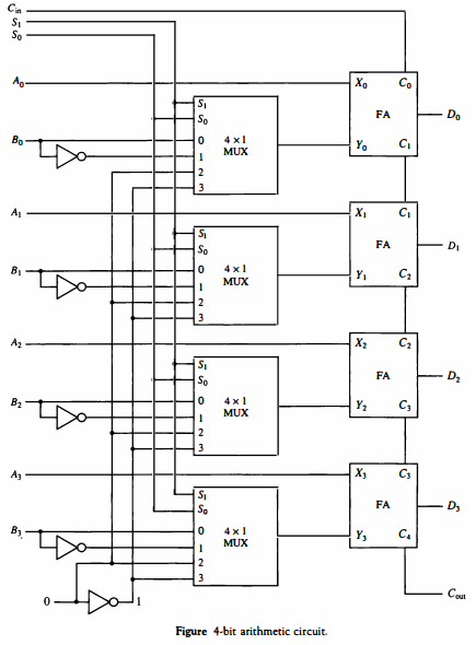
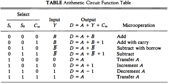
When S1S0 = 00, the value of B is applied to the Y inputs of the adder. If Cin = 0, the output D = A + B . If Cin = 1, output D = A + B + l. Both cases perform the add microoperation with or without adding the input carry.
When S1S0 = 01, the complement of B is applied to the Y inputs of the adder. If Cin = 1, then D = A + B + 1. This produces A plus the 2's complement of B, which is equivalent to a subtraction of A - B.
When Cin = 0, then D = A + B. This is equivalent to a subtract with borrow, that is, A - B - 1. When S1S0 = 10, the inputs from B are neglected, and instead, all O's are inserted into the Y inputs. The output becomes D = A + 0 + Cm· This gives D = A when Cin = 0 and D = A + 1 when Cin = 1. In the first case we have a direct transfer from input A to output D.
In the second case, the value of A is incremented by 1. When S1S0 = 11, all 1' s are inserted into the Y inputs of the adder to produce the decrement operation D = A - 1 when Cin = 0.
This is because a number with all 1's is equal to the 2's complement of 1 (the 2's complement of binary 0001 is 1111). Adding a number A to the 2's complement of 1 produces F = A + 2's complement of 1 = A - 1. When Cin = 1, then D = A - 1 + 1 = A, which causes a direct transfer from input A to output D.
Note that the microoperation D = A is generated twice, so there are only seven distinct microoperations in the arithmetic circuit.