Logic Microoperations
Logic microoperations specify binary operations for strings of bits stored in registers.
These operations consider each bit of the register separately and treat them as binary variables.
For example, the exclusive-OR microoperation with the contents of two registers R 1 and R2 is symbolized by the statement P: R1 ← R1 ⊕ R2
It specifies a logic microoperation to be executed on the individual bits of the registers provided that the control variable P = 1. As a numerical example, assume that each register has four bits. Let the content of R1 be 1010 and the content of R2 be 1100.
The exclusive-OR microoperation stated above symbolizes the following logic computation:
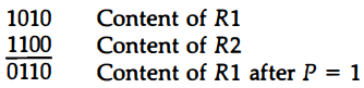
The content of R1, after the execution of the microoperation, is equal to the bit-by-bit exclusive-OR operation on pairs of bits in R2 and previous values of R1. The logic microoperations are seldom used in scientific computations, but they are very useful for bit manipulation of binary data and for making logical decisions.
Special symbols will be adopted for the logic microoperations OR, AND, and complement, to distinguish them from the corresponding symbols used to express Boolean functions.
The symbol V will be used to denote an OR microoperation and the symbol ∧ to denote an AND microoperation. The complement microoperation is the same as the 1's complement and uses a bar on top of the symbol that denotes the register name.
By using different symbols, it will be possible to differentiate between a logic microoperation and a control (or Boolean) function.
Another reason for adopting two sets of symbols is to be able to distinguish the symbol + , when used to symbolize an arithmetic plus, from a logic OR operation.
Although the + symbol has two meanings, it will be possible to distinguish between them by noting where the symbol occurs. When the symbol + occurs in a microoperation, it will denote an arithmetic plus.
When it occurs in a control (or Boolean) function, it will denote an OR operation. We will never use it to symbolize an OR microoperation.
For example, in the statement P + Q: R1 ← R2 + R3, R4 ← R5 ∨ R6 the + between P and Q is an OR operation between two binary variables of a control function.
The + between R2 and R3 specifies an add microoperation. The OR microoperation is designated by the symbol V between registers R5 and R6.
List of Logic Microoperations
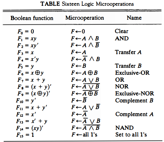
There are 16 different logic operations that can be performed with two binary variables.
They can be determined from all possible truth tables obtained with two binary variables as shown in Table below.
In this table, each of the 16 columns F0 through F15 represents a truth table of one possible Boolean function for the
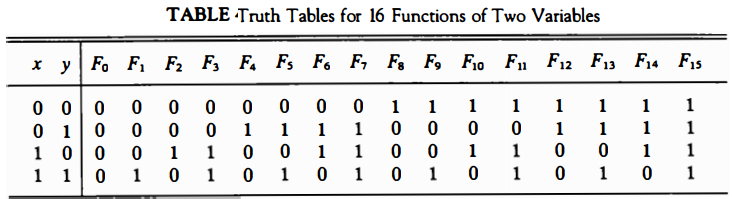 two variables x and y.
Note that the functions are determined from the 16 binary combinations that can be assigned to F. The 16 Boolean functions of two variables x and y are expressed in algebraic form in the first column of Table below.
The 16 logic microoperations are derived from these functions by replacing variable x by the binary content of register A and variable y by the binary content of register B.
It is important to realize that the Boolean functions listed in the first column of Table below represent a relationship between two binary variables x and y.
The logic microoperations listed in the second column represent a relationship between the binary content of two registers A and B.
Each bit of the register is treated as a binary variable and the microoperation is performed on the string of bits stored in the registers.
Hardware Implementation
The hardware implementation of logic rnicrooperations requires that logic gates be inserted for each bit or pair of bits in the registers to perform the required logic function.
Although there are 16 logic rnicrooperations, most computers use only four-AND, OR, XOR (exclusive-OR), and complement from which all others can be derived.
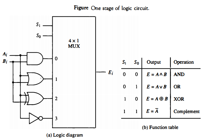
Figure below shows one stage of a circuit that generates the four basic logic rnicrooperations .
It consists of four gates and a multiplexer. Each of the four logic operations is generated through a gate that performs the required logic.
The outputs of the gates are applied to the data inputs of the multiplexer. The two selection inputs S1 and S0 choose one of the data inputs of the multiplexer and direct its value to the output.
The diagram shows one typical stage with subscript i. For a logic circuit with n bits, the diagram must be repeated n times for i = 0, 1, 2, ... , n - 1.
The selection variables are applied to all stages. The function table in Fig. below lists the logic rnicrooperations obtained for each combination of the selection variables.
Some Applications
Logic microoperations are very useful for manipulating individual bits or a portion of a word stored in a register.
They can be used to change bit values, delete a group of bits, or insert new bit values into a register. The following examples show how the bits of one register (designated by A) are manipulated
by logic microoperations as a function of the bits of another register (designated by B).
In a typical application, register A is a processor register and the bits of register B constitute a logic operand extracted from memory and placed in register B.
The selective-set operation sets to 1 the bits in register A where there are corresponding 1's in register B. It does not affect bit positions that have 0's in B.
The following numerical example clarifies this operation:
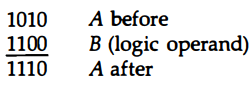
The two leftmost bits of B are 1' s, so the corresponding bits of A are set to 1.
One of these two bits was already set and the other has been changed from 0 to 1. The two bits of A with corresponding 0' s in B remain unchanged. The example above serves as a truth table since it has all four possible combinations of two binary variables.
From the truth table we note that the bits of A after the operation are obtained from the logic-OR operation of bits in B and previous values of A. Therefore, the OR rnicrooperation can be used to selectively set bits of a register.
The selective-complement operation complements bits in A where there are selective-clear corresponding 1's in B. It does not affect bit positions that have 0's in B. For example:
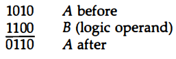
Again the two leftmost bits of B are 1's, so the corresponding bits of A are complemented.
This example again can serve as a truth table from which one can deduce that the selective-complement operation is just an exclusive-OR microoperation.
Therefore, the exclusive-OR rnicrooperation can be used to selectively complement bits of a register.
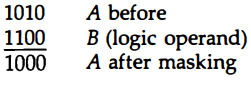
The selective-clear operation clears to 0 the bits in A only where there are corresponding 1's in B. For example:
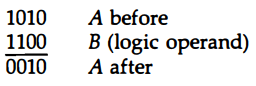
Again the two leftmost bits of B are 1' s, so the corresponding bits of A are cleared to 0.
One can deduce that the Boolean operation performed on the individual bits is AB'. The corresponding logic microoperation is A ← A ∧ B
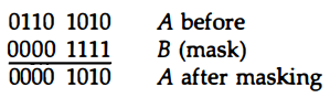
The mask operation is similar to the selective-clear operation except that the bits of A are cleared only where there are corresponding 0's in B. The mask operation is an AND micro operation as seen from the following numerical example:
The two rightmost bits of A are cleared because the corresponding bits of B are 0' s. The two leftmost bits are left unchanged because the corresponding bits of B are 1's.
The mask operation is more convenient to use than the selective clear operation because most computers provide an AND instruction, and few provide an instruction that executes the microoperation for selective-clear.
The insert operation inserts a new value into a group of bits. This is done by first masking the bits and then ORing them with the required value. For example, suppose that an A register contains eight bits, 0110 1010.
To replace the four leftmost bits by the value 1001 we first mask the four unwanted bits:
and then insert the new value:
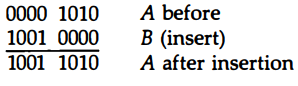
The mask operation is an AND microoperation and the insert operation is an OR microoperation.
The clear operation compares the words in A and B and produces an all 0' s result if the two numbers are equal. This operation is achieved by an exclusive-OR microoperation as shown by the following example:
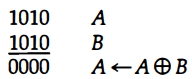
When A and B are equal, the two corresponding bits are either both 0 or both 1. In either case the exclusive-OR operation produces a 0. The all-0's result is then checked to determine if the two numbers were equal.
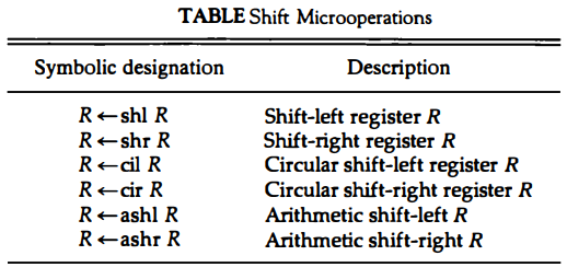
Shift Microoperations
Shift microoperations are used for serial transfer of data. They are also used in conjunction with arithmetic, logic, and other data-processing operations.
The contents of a register can be shifted to the left or the right. At the same time that the bits are shifted, the first flip-flop receives its binary information from the serial input.
During a shift-left operation the serial input transfers a bit into the rightmost position.
During a shift-right operation the serial input transfers a bit into the leftmost position.
The information transferred through the serial input determines the type of shift.
There are three types of shifts: logical, circular, and arithmetic.
A logical shift is one that transfers 0 through the serial input. We will adopt the symbols shl and shr for logical shift-left and shift-right microoperations. For example:
R1 ← shl R1
R2 &arr; shr R2
are two microoperations that specify a 1-bit shift to the left of the content of register R 1 and a 1-bit shift to the right of the content of register R2. The register symbol must be the same on both sides of the arrow.
The bit transferred to the end position through the serial input is assumed to be 0 during a logical shift. The circular shift (also known as a rotate operation) circulates the bits of the register around the two ends without loss of information.
This is accomplished by connecting the serial output of the shift register to its serial input.
We will use the symbols cil and cir for the circular shift left and right, respectively. The symbolic notation for the shift rnicrooperations is shown in Table below.
An arithmetic shift is a microoperation that shifts a signed binary number to the left or right. An arithmetic shift-left multiplies a signed binary number by 2. An arithmetic shift-right divides the number by 2.
Arithmetic shifts must leave the sign bit unchanged because the sign of the number remains the same
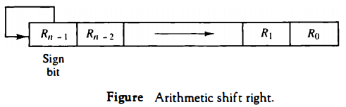
when it is multiplied or divided by 2. The leftmost bit in a register holds the sign bit, and the remaining bits hold the number. The sign bit is 0 for positive and I for negative. Negative numbers are in 2's complement form.
Figure above shows a typical register of n bits. Bit Rn-1 in the leftmost position holds the sign bit. Rn-2 is the most significant bit of the number and R0 is the least significant bit.
The arithmetic shift-right leaves the sign bit unchanged and shifts the number (including the sign bit) to the right.
Thus Rn-1 remains the same, Rn-2 receives the bit from Rn-1 and so on for the other bits in the register. The bit in R0 is lost.
The arithmetic shift-left inserts a 0 into R0, and shifts all other bits to the left. The initial bit of Rn-1 is lost and replaced by the bit from Rn-2. A sign reversal occurs if the bit in Rn-1 changes in value after the shift.
This happens if the multiplication by 2 causes an overflow. An overflow occurs after an arithmetic shift left if initially, before the shift, Rn-1 is not equal to Rn-2.
An overflow flip-flop Vs, can be used to detect an arithmetic shift-left overflow. Vs = Rn-1 ⊕ Rn-2
If Vs = 0, there is no overflow, but if Vs = 1, there is an overflow and a sign reversal after the shift. Vs must be transferred into the overflow flip-flop with the same clock pulse that shifts the register.
Hardware Implementation
A possible choice for a shift unit would be a bidirectional shift register with parallel load
Information can be transferred to the register in parallel and then shifted to the right or left.
In this type of configuration, a clock pulse is needed for loading the data into the register, and another pulse is needed to initiate the shift.
In a processor unit with many registers it is more efficient to implement the shift operation with a combinational circuit.
In this way the content of a register that has to be shifted is first placed onto a common bus whose output is connected to the combinational shifter, and the shifted number is then loaded back into the register.
This requires only one clock pulse for loading the shifted value into the register.
A combinational circuit shifter can be constructed with multiplexers as shown in Fig. below. The 4-bit shifter has four data inputs, A0 through A3, and four data outputs, H0 through H3.
There are two serial inputs, one for shift left
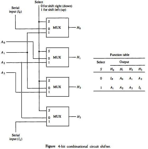
(IL) and the other for shift right (IL). When the selection input S = 0, the input data are shifted right (down in the diagram). When S = 1, the input data are shifted left (up in the diagram). The function table in Fig. above shows which input goes to each output after the shift.
A shifter with n data inputs and outputs requires n multiplexers. The two serial inputs can be controlled by another multiplexer to provide the three possible types of shifts.
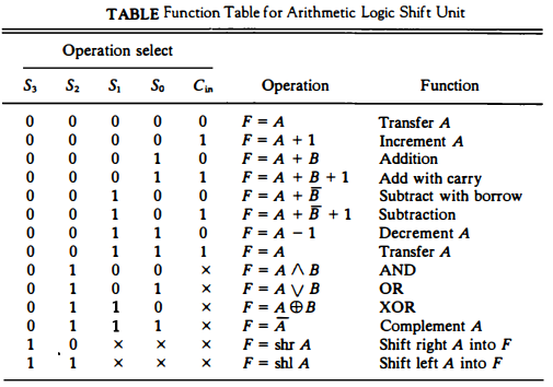
Arithmetic Logic Shift Unit
Instead of having individual registers performing the microoperations directly, computer systems employ a number of storage registers connected to a common operational unit called an arithmetic logic unit, abbreviated ALU.
To perform a microoperation, the contents of specified registers are placed in the inputs of the common ALU.
The ALU performs an operation and the result of the operation is then transferred to a destination register.
The ALU is a combinational circuit so that the entire register transfer operation from the source registers through the ALU and into the destination register can be performed during one clock pulse period.
The shift microoperations are often performed in a seperate unit, but sometimes the shift unit is made part of the ALU.
The arithmetic, logic, and shift circuits introduced in previous sections can be combined into one ALU with common selection variables.
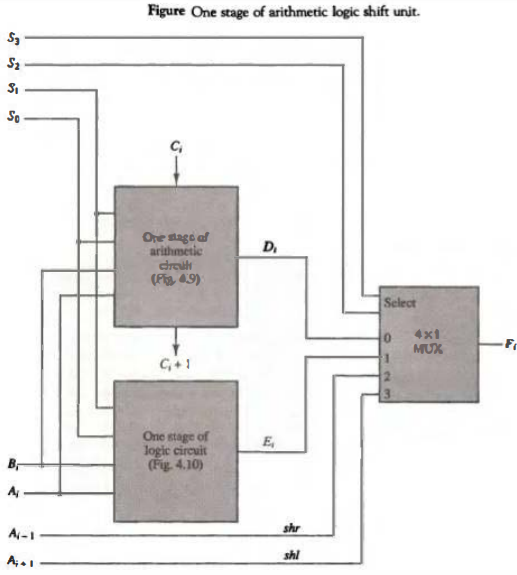
One stage of an arithmetic logic shift unit is shown in Fig. below. The subscript i designates a typical stage.
Inputs Ai and Bi are applied to both the arithmetic and logic
 units.
A particular microoperation is selected with inputs S1 and S0. A 4 x 1 multiplexer at the output chooses between an arithmetic output in Ei and a logic output in Hi.
The data in the multiplexer are selected with inputs S3 and S2.
The other two data inputs to the multiplexer receive inputs Ai-1 for the shift-right operation and Ai+1 for the shift-left operation. Note that the diagram shows just one typical stage.
The circuit of Fig. below must be repeated n times for an n-bit ALU. The output carry Ci+1 of a given arithmetic stage must be connected to the input carry Ci of the next stage in sequence. The input carry to the first stage is the input carry Cin which provides a selection variable for the arithmetic operations.
The circuit whose one stage is specified in Fig. above provides eight arithmetic operation, four logic operations, and two shift operations.
Each operation is selected with the five variables S3, S2, S1, S0, and Cin.
The input carry Cin is used for selecting an arithmetic operation only.
Table below lists the 14 operations of the ALU.
The first eight are arithmetic operations and are selected with S3S2 = 00. The next four are logic operations and are selected with S3S2 = 01. The input carry has no effect during the logic operations and is marked with don't-care x's.
The last two operations are shift operations and are selected with S3S2 = 10 and 11. The other three selection inputs have no effect on the shift.