Common Bus System
The basic computer has eight registers, a memory unit, and a control unit . Paths must be provided to transfer information from one register to another and between memory and registers.
The number of wires will be excessive if connections are made between the outputs of each register and the inputs of the other registers.
A more efficient scheme for transferring information in a system with many registers is to use a common bus.
The connection of the registers and memory of the basic computer to a common bus system is shown in Fig. below. The outputs of seven registers and memory are connected to the common bus.
The specific output that is selected for the bus lines at any given time is determined from the binary value of the selection variables S2, S1, and S0.
The number along each output shows the decimal equivalent of the required binary selection. For example, the number along the output of DR is 3.
The 16-bit outputs of DR are placed on the bus lines when S2S1S0 = 011 since this is the binary value of decimal 3.
The lines from the common bus are connected to the inputs of each register and the data inputs of the memory. The particular register whose LD (load) input is enabled receives the data from the bus during the next clock pulse transition.
The memory receives the contents of the bus when its write input is activated. The memory places its 16-bit output onto the bus when the read input is activated and S2S1S0 = 111.
Four registers, DR, AC, IR, and TR, have 16 bits each. Two registers, AR
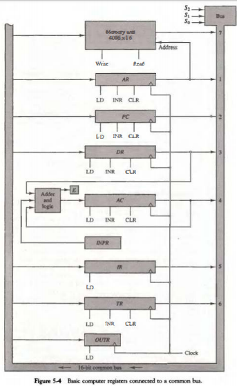
and PC, have 12 bits each since they hold a memory address. When the contents of AR or PC are applied to the 16-bit common bus, the four most significant bits are set to 0's.
When AR or PC receive information from the bus, only the 12 least significant bits are transferred into the register. The input register INPR and the output register OUTR have 8 bits each and communicate with the eight least significant bits in the bus.
INPR is connected to provide information to the bus but OUTR can only receive information from the bus.
This is because INPR receives a character from an input device which is then transferred to AC. OUTR receives a character from AC and delivers it to an output device. There is no transfer from OUTR to any of the other registers.
The 16 lines of the common bus receive information from six registers and the memory unit. The bus lines are connected to the inputs of six registers and the memory. Five registers have three control inputs: LD (load), INR (increment), and CLR (clear).
This type of register is equivalent to a binary counter with parallel load and synchronous clear. The increment operation is achieved by enabling the count input of the counter. Two registers have only a LD input.
The input data and output data of the memory are connected to the common bus, but the memory address is connected to AR. Therefore, AR must always be used to specify a memory address.
By using a single register for the address, we eliminate the need for an address bus that would have been needed otherwise. The content of any register can be specified for the memory data input during a write operation. Similarly, any register can receive the data from memory after a read operation except AC .
The 16 inputs of AC come from an adder and logic circuit. This circuit has three sets of inputs. One set of 16-bit inputs come from the outputs of AC . They are used to implement register microoperations such as complement AC and shift AC .
Another set of 16-bit inputs come from the data register DR. The inputs from DR and AC are used for arithmetic and logic rnlcrooperations, such as add DR to AC or AND DR to AC.
The result of an addition is transferred to AC and the end carry-out of the addition is transferred to flip-flop E (extended AC bit). A third set of 8-bit inputs come from the input register INPR.
Note that the content of any register can be applied onto the bus and an operation can be performed in the adder and logic circuit during the same clock cycle. The clock transition at the end of the cycle transfers the content of the bus into the designated destination register and the output of the adder and logic circuit into AC.
For example, the two microoperations
DR ← AC and AC ← DR
can be executed at the same time. This can be done by placing the content of AC on the bus (with S2S1S0 = 100), enabling the LD (load) input of DR, transferring the content of DR through the adder and logic circuit into AC, and enabling the LD (load) input of AC, all during the same clock cycle.
The two transfers occur upon the arrival of the clock pulse transition at the end of the clock cycle.
Computer Instructions
The basic computer has three instruction code formats, as shown in Fig. below. Each format has 16 bits.
The operation code (opcode) part of the instruction contains three bits and the meaning of the remaining 13 bits depends on the operation code encountered.
A memory-reference instruction uses 12 bits to specify an address and one bit to specify the addressing mode I. I is equal to 0 for direct address and to 1 for indirect address.
The register reference instructions are recognized by the operation code 111 with a 0 in the leftmost bit (bit 15) of the instruction.
A register-reference instruction specifies an operation on or a test of the AC register. An operand from memory is not needed; therefore, the other 12 bits are used to specify the operation or test to be executed.
Similarly, an input-output instruction does not need a reference to memory and is recognized by the operation code Ill with a 1 in the leftmost bit of the instruction. The remaining 12 bits are used to specify the type of input-output operation or test performed.
The type of instruction is recognized by the computer control from the four bits in positions 12 through 15 of the instruction. If the three opcode bits in positions 12 though 14 are not equal to 111, the instruction is a memory-reference type and the bit in position 15 is taken as the addressing mode I.
If the 3-bit opcode is equal to 111, control then inspects the bit in position 15. If this bit is 0, the
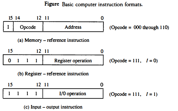
instruction is a register-reference type. If the bit is 1, the instruction is an input-output type. Note that the bit in position 15 of the instruction code is designated by the symbol I but is not used as a mode bit when the operation code is equal to 111.
Only three bits of the instruction are used for the operation code. It may seem that the computer is restricted to a maximum of eight distinct operations.
However, since register-reference and input-output instructions use the remaining 12 bits as part of the operation code, the total number of instructions can exceed eight.
In fact, the total number of instructions chosen for the basic computer is equal to 25.
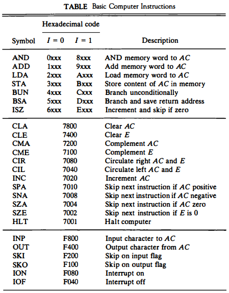
The instructions for the computer are listed in Table below. The symbol designation is a three-letter word and represents an abbreviation intended for programmers and users. The hexadecimal code is equal to the equivalent hexadecimal number of the binary code used for the instruction.
By using the hexadecimal equivalent we reduced the 16 bits of an instruction code to four digits with each hexadecimal digit being equivalent to four bits.
A memory-reference instruction has an address part of 12 bits. The address part is denoted by three x's and stand for the three hexadecimal digits corresponding to the 12-bit address.
The last bit of the instruction is designated by the symbol I. When I = 0, the last four bits of an instruction have a hexadecimal digit equivalent from 0 to 6 since the last bit is 0.
When I = I, the hexadecimal digit equivalent of the last four bits of the instruction ranges from 8 to E since the last bit is I. Register-reference instructions use 16 bits to specify an operation. The leftmost four bits are always 0111, which is equivalent to hexadecimal 7.
The other three hexadecimal digits give the binary equivalent of the remaining 12 bits. The input-output instructions also use all 16 bits to specify an operation. The last four bits are always 1111, equivalent to hexadecimal F.
Instruction Set Completeness
A computer should have a set of instructions so that the user can construct machine language programs to evaluate any function that is known to be computable.
The set of instructions are said to be complete if the computer includes a sufficient number of instructions in each of the following categories:
1. Arithmetic, logical, and shift instructions
2. Instructions for moving information to and from memory and processor
registers
3. Program control instructions together with instructions that check
status conditions
4. Input and output instructions
Arithmetic, logical, and shift instructions provide computational capabilities for processing the type of data that the user may wish to employ.
The bulk of the binary information in a digital computer is stored in memory, but all computations are done in processor registers.
Therefore, the user must have the capability of moving information between these two units. Decision making capabilities are an important aspect of digital computers.
For example, two numbers can be compared, and if the first is greater than the second, it may be necessary to proceed differently than if the second is greater than the first.
Program control instructions such as branch instructions are used to change the sequence in which the program is executed. Input and output instructions are needed for communication between the computer and the user.
Programs and data must be transferred into memory and results of computations must be transferred back to the user. The instructions listed in Table above constitute a minimum set that provides all the capabilities mentioned above.
There is one arithmetic instruction, ADD, and two related instructions, complement AC(CMA) and increment AC(INC).
With these three instructions we can add and subtract binary numbers when negative numbers are in signed-2's complement representation. The circulate instructions, CIR and CIL, can be used for arithmetic shifts as well as any other type of shifts desired.
Multiplication and division can be performed using addition, subtraction, and shifting. There are three logic operations: AND, complement AC(CMA), and clear AC(CLA).
The AND and complement provide a NAND operation. It can be shown that with the NAND operation it is possible to implement all the other logic operations with two variables.
Moving information from memory to AC is accomplished with the load AC(LDA) instruction. Storing information from AC into memory is done with the store AC(STA) instruction.
The branch instructions BUN, BSA, and ISZ, together with the four skip instructions, provide capabilities for program control and checking of status conditions. The input (lNP) and output (OUT) instructions cause information to be transferred between the computer and external devices.
Although the set of instructions for the basic computer is complete, it is not efficient because frequently used operations are not performed rapidly. An efficient set of instructions will include such instructions as subtract, multiply, OR, and exclusive-OR.
Timing and Control
The timing for all registers in the basic computer is controlled by a master clock generator.
The clock pulses are applied to all flip-flops and registers in the system, including the flip-flops and registers in the control unit.
The clock pulses do not change the state of a register unless the register is enabled by a control signal.
The control signals are generated in the control unit and provide control inputs for the multiplexers in the common bus, control inputs in processor registers, and microoperations for the accumulator.
There are two major types of control organization: hardwired control and microprogrammed control. In the hardwired organization, the control logic is implemented with gates, flip-flops, decoders, and other digital circuits.
It has the advantage that it can be optimized to produce a fast mode of operation.
In the microprogrammed organization, the control information is stored in a control memory. The control memory is programmed to initiate the required sequence of microoperations.
A hardwired control, as the name implies, requires changes in the wiring among the various components if the design has to be modified or changed. In the microprogrammed control, any required changes or modifications can be done by updating the microprogram in control memory.
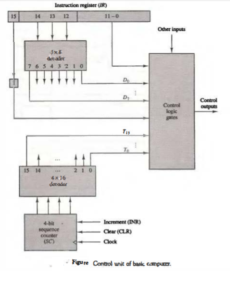
The block diagram of the control unit is shown in Fig. below. It consists of two decoders, a sequence counter, and a number of control logic gates. An instruction read from memory is placed in the instruction register (IR).
The position of this register in the common bus system is indicated in Fig. previously seen. The instruction register is shown again in Fig. below, where it is divided into three parts: the I bit, the operation code, and bits 0 through 11.
The operation code in bits 12 through 14 are decoded with a 3 x 8 decoder. The eight outputs of the decoder are designated by the symbols D0 through D7
The subscripted decimal number is equivalent to the binary value of the corresponding operation code. Bit 15 of the instruction is transferred to a flip-flop designated by the symbol I.
Bits 0 through 11 are applied to the control logic gates. The 4-bit sequence counter can count in binary from 0 through 15. The outputs of the counter are decoded into 16 timing signals T0 through T15
The sequence counter SC can be incremented or cleared synchronously
. Most of the time, the counter is incremented to provide the sequence of timing signals out of the 4 x 16 decoder. Once in awhile, the counter is cleared to 0, causing the next active timing signal to be T0.
As an example, consider the case where SC is incremented to provide timing signals T0, T1, T2, T3, and T4 in sequence. At time T4, SC is cleared to 0 if decoder output D3 is active.
This is expressed symbolically by the statement D3T4: SC ← 0. The timing diagram of Fig. below shows the time relationship of the control signals.
The sequence counter SC responds to the positive transition of the clock. Initially, the CLR input of SC is active. The first positive transition of the
clock clears SC to 0, which in turn activates the timing signal T0 out of the decoder. T0 is active during one clock cycle.
The positive clock transition labeled T0 in the diagram will trigger only those registers whose control inputs are connected to timing signal T0.
SC is incremented with every positive clock unless its CLR input is active.
This produces the sequence of timing signals \( T_0, T_1, T_2, T_3, T_4 \) and so on, as shown in the diagram. (Note the relationship between the timing signal and its corresponding positive clock transition.)
If SC is not cleared, the timing signals will continue with T5, T6 up to T15 and back to T0.
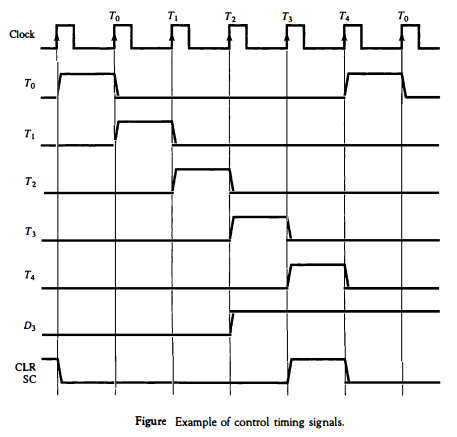
The last three waveforms in Fig. above show how SC is cleared when D3T4 = 1. Output D3 from the operation decoder becomes active at the end of timing signal T2
When timing signal T4 becomes active, the output of the AND gate that implements the control function D3T4 becomes active.
This signal is applied to the CLR input of SC. On the next positive clock transition (the one marked T4 in the diagram) the counter is cleared to 0. This causes the timing signal T0 to become active instead of T5 that would have been active if SC were incremented instead of cleared.
A memory read or write cycle will be initiated with the rising edge of a timing signal. It will be assumed that a memory cycle time is less than the clock cycle time. According to this assumption, a memory read or write cycle initiated by a timing signal will be completed by the time the next clock goes through its positive transition.
The clock transition will then be used to load the memory word into a register. This timing relationship is not valid in many computers because the memory cycle time is usually longer than the processor clock cycle.
In such a case it is necessary to provide wait cycles in the processor until the memory word is available. To facilitate the presentation, we will assume that a wait period is not necessary in the basic computer.
To fully comprehend the operation of the computer, it is crucial that one understands the timing relationship between the clock transition and the timing signals. For example, the register transfer statement T0: AR ← PC specifies a transfer of the content of PC into AR if timing signal T0 is active.
T0 is active during an entire clock cycle interval. During this time the content of PC is placed onto the bus (with S2S1S0 = 010) and the LD (load) input of AR is enabled. The actual transfer does not occur until the end of the clock cycle when the clock goes through a positive transition.
This same positive clock transition increments the sequence counter SC from 0000 to 0001 . The next clock cycle has T1 active and T0 inactive.