Instruction Cycle
A program residing in the memory unit of the computer consists of a sequence of instructions. The program is executed in the computer by going through a cycle for each instruction. Each instruction cycle in turn is subdivided into a sequence of subcycles or phases. In the basic computer each instruction cycle consists of the following phases:
1. Fetch an instruction from memory.
2. Decode the instruction.
3. Read the effective address from memory if the instruction has an indirect
address.
4. Execute the instruction.
Upon the completion of step 4, the control goes back to step 1 to fetch, decode, and execute the next instruction. This process continues indefinitely unless a HALT instruction is encountered.
Fetch and Decode
Initially, the program counter PC is loaded with the address of the first instruction in the program.
The sequence counter SC is cleared to 0, providing a decoded timing signal T0. After each clock pulse, SC is incremented by one, so that the timing signals go through a sequence T0, T1, T2, and so on.
The rnicrooperations for the fetch and decode phases can be specified by the following register transfer statements.
T0: AR ← PC
T1: IR ← M[AR], PC ← PC + 1
T2: D0, .... , D7 ← Decode IR(12-14), AR ← IR(0-11), I ← IR(15)
Since only AR is connected to the address inputs of memory, it is necessary to transfer the address from PC to AR during the clock transition associated with timing signal T0. The instruction read from memory is then placed in the instruction register IR with the clock transition associated with timing signal T1.
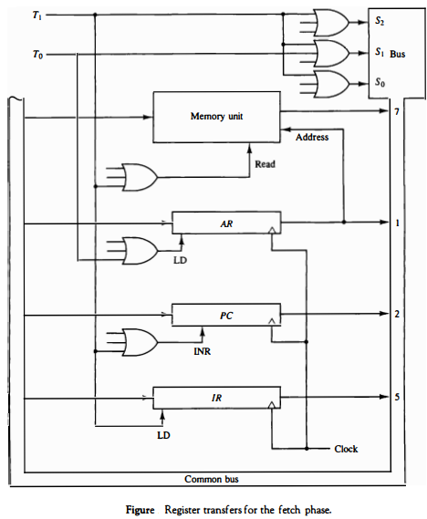
At the same time, PC is incremented by one to prepare it for the address of the next instruction in the program. At time T2, the operation code in IR is decoded, the indirect bit is transferred to flip-flop I, and the address part of the instruction is transferred to AR .
Note that SC is incremented after each clock pulse to produce the sequence T0, T1, and T2
Figure above shows how the first two register transfer statements are implemented in the bus system.
To provide the data path for the transfer of PC to AR we must apply timing signal T0 to achieve the following connection:
1. Place the content of PC onto the bus by making the bus selection inputs
S2S1S0 equal to 010.

2. Transfer the content of the bus to AR by enabling the LD input of AR .
The next clock transition initiates the transfer from PC to AR since T0 = 1. In order to implement the second statement : T1: IR ← M[AR], PC ← PC + 1 it is necessary to use timing signal T1 to provide the following connections in the bus system.
1. Enable the read input of memory.
2. Place the content of memory onto the bus by making S2S1S0 = 111.
3. Transfer the content of the bus to IR by enabling the LD input of IR.
4. Increment PC by enabling the INR input of PC.
The next clock transition initiates the read and increment operations since T1 = 1.
Figure above duplicates a portion of the bus system and shows how T0 and T1 are connected to the control inputs of the registers, the memory, and the bus selection inputs. Multiple input OR gates are included in the diagram because there are other control functions that will initiate similar operations.
Determine the Type of Instruction
The timing signal that is active after the decoding is T3. During time T3, the control unit determines the type of instruction that was just read from memory.
The flowchart of Fig. below presents an initial configuration for the instruction cycle and shows how the control determines the instruction type after the decoding.
The three possible instruction types available in the basic computer are specified in Fig. on basic computer formats.
Decoder output D7 is equal to 1 if the operation code is equal to binary 111. From Fig. on basic computer formats we determine that if D7 = 1, the instruction must be a
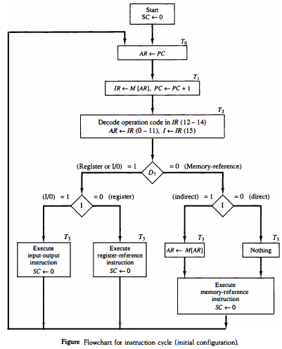 register-reference or input-output type.
If D7 = 0, the operation code must be one of the other seven values 000 through 110, specifying a memory-reference instruction.
Control then inspects the value of the first bit of the instruction, which is now available in flip-flop I. If D7 = 0 and I = 1, we have a memory reference instruction with an indirect address.
It is then necessary to read the effective address from memory. The microoperation for the indirect address condition can be symbolized by the register transfer statement : AR ← M[AR]
Initially, AR holds the address part of the instruction. This address is used during the memory read operation. The word at the address given by AR is read from memory and placed on the common bus. The LD input of AR is then enabled to receive the indirect address that resided in the 12 least significant bits of the memory word.
The three instruction types are subdivided into four separate paths. The selected operation is activated with the clock transition associated with timing signal T3. This can be symbolized as follows:
D'7 IT3: AR ← M[AR]
D'7 I'T3: Nothing
D7 I'T3: Execute a register-reference instruction
D7IT3: Execute an input-output instruction
When a memory-reference instruction with I = 0 is encountered, it is not necessary to do anything since the effective address is already in AR.
However, the sequence counter SC must be incremented when D'7T3 = 1, so that the execution of the memory-reference instruction can be continued with timing variable T4
A register-reference or input-output instruction can be executed with the clock associated with timing signal T3. After the instruction is executed, SC is cleared to 0 and control returns to the fetch phase with T0 = 1.
Note that the sequence counter SC is either incremented or cleared to 0 with every positive clock transition. We will adopt the convention that if SC is incremented, we will not write the statement SC ← SC + 1, but it will be implied that the control goes to the next timing signal in sequence. When SC is to be cleared, we will include the statement SC ← 0.
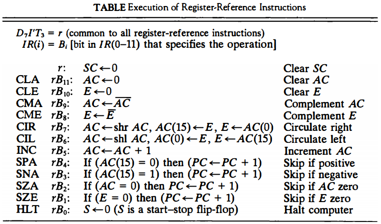
The register transfers needed for the execution of the register-reference instructions are presented in this section.
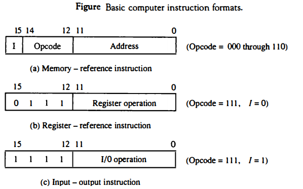
Register-Reference Instructions
Register-reference instructions are recognized by the control when D7 = 1 and I = 0.
These instructions use bits 0 through 11 of the instruction code to specify one of 12 instructions.
These 12 bits are available in IR(0-11). They were also transferred to AR during time T2.
The control functions and microoperations for the register-reference instructions are. listed in Table below. These instructions are executed with the clock transition associated with timing variable T3.
Each control function needs the Boolean relation D7I'T3, which we designate for convenience by the symbol r.
The control function is distinguished by one of the bits in IR(0-11). By assigning the symbol Bi to bit i of IR, all control functions can be simply denoted by rBi.
For example, the instruction CLA has the hexadecimal code 7800, which gives the binary equivalent 0111 1000 0000 0000. The first bit is a zero and is equivalent to I'.
The next three bits constitute the operation code and are recognized from decoder output D7. Bit 11 in IR is I and is recognized from B11. The control function that initiates the microoperation for this instruction is D7I'T3B11 = rB11.
The execution of a register-reference instruction is completed at time T3.
The sequence counter SC is cleared to 0 and the control goes back to fetch the next instruction with timing signal T0.
The first seven register-reference instructions perform clear, complement, circular shift, and increment microoperations on the AC or E registers.
The next four instructions cause a skip of the next instruction in sequence when a stated condition is satisfied. The skipping of the instruction is achieved by incrementing PC once again (in addition, it is being incremented during the fetch phase at time T1).
The condition control statements must be recognized as part of the control conditions .
The AC is positive when the sign bit in AC(15) = 0; it is negative when AC(15) = 1. The content of AC is zero (AC = 0) if all the flip-flops of the register are zero. The HLT instruction clears a start-stop flip-flop S and stops the sequence counter from counting. To restore the operation of the computer, the start-stop flip-flop must be set manually.
Memory-Reference Instructions
In order to specify the rnicrooperations needed for the execution of each instruction, it is necessary that the function that they are intended to perform be defined precisely.
We will now show that the function of the memory-reference instructions can be defined precisely by means of register transfer notation.
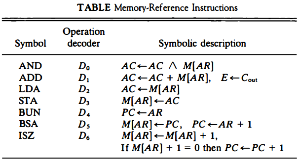
Table below lists the seven memory-reference instructions. The decoded output Di for i = 0, 1, 2, 3, 4, 5, and 6 from the operation decoder that belongs to each instruction is included in the table.
The effective address of the instruction is in the address register AR and was placed there during timing signal T2 when I = 0, or during timing signal T3 when I = 1.
The execution of the memory-reference instructions starts with timing signal T4. The symbolic description of each instruction is specified in the table in terms of register transfer notation.
The actual execution of the instruction in the bus system will require a sequence of microoperations.
This is because data stored in memory cannot be processed directly.
The data must be read from memory to a register where they can be operated on with logic circuits.
We now explain the operation of each instruction and list the control functions and microoperations needed for their execution.
AND to AC
This is an instruction that performs the AND logic operation on pairs of bits in AC and the memory word specified by the effective address.
The result of the operation is transferred to AC. The microoperations that execute this instruction are:
D0T4: DR ← M[AR]
D0T5: AC ← AC ∧ DR, SC ← 0The control function for this instruction uses the operation decoder D0 since this output of the decoder is active when the instruction has an AND operation whose binary code value is 000. Two timing signals are needed to execute the instruction.
The clock transition associated with timing signal T4 transfers the operand from memory into DR.
The clock transition associated with the next timing signal T5 transfers to AC the result of the AND logic operation between the contents of DR and AC.
The same clock transition clears SC to 0, transferring control to timing signal T0 to start a new instruction cycle.
ADD to AC
This instruction adds the content of the memory word specified by the effective address to the value of AC.
The sum is transferred into AC and the output carry Cout is transferred to the E (extended accumulator) flip-flop.
The microoperations needed to execute this instruction are
D1T4: DR ← M[AR]
D1T5: AC ← AC + DR, E ← Cout, SC ← 0The same two timing signals, T4 and T5, are used again but with operation decoder D1 instead of D0, which was used for the AND instruction.
After the instruction is fetched from memory and decoded, only one output of the operation decoder will be active, and that output determines the sequence of rnicrooperations that the control follows during the execution of a memory-reference instruction.
LDA: Load to AC
This instruction transfers the memory word specified by the effective address to AC.
The microoperations needed to execute this instruction are
D2T4: DR ← M [AR]
D2T5: AC ← DR, SC ← 0Note that there is no direct path from the bus into AC (see figure under Common Bus System).
The adder and logic circuit receive information from DR which can be transferred into AC.
Therefore, it is necessary to read the memory word into DR first and then transfer the content of DR into AC.
The reason for not connecting the bus to the inputs of AC is the delay encountered in the adder and logic circuit.
It is assumed that the time it takes to read from memory and transfer the word through the bus as well as the adder and logic circuit is more than the time of one clock cycle.
By not connecting the bus to the inputs of AC we can maintain one clock cycle per rnicrooperation.
STA: Store AC
This instruction stores the content of AC into the memory word specified by the effective address. Since the output of AC is applied to the bus and the data input of memory is connected to the bus, we can execute this instruction with one microoperation:
D3T4: M [AR] ← AC, SC ← 0
BUN: Branch Unconditionally
This instruction transfers the program to the instruction specified by the effective address.
Remember that PC holds the address of the instruction to be read from memory in the next instruction cycle.
PC is incremented at time T1 to prepare it for the address of the next instruction in the program sequence.
The BUN instruction allows the programmer to specify an instruction out of sequence and we say that the program branches (or jumps) unconditionally.
The instruction is executed with one microoperation:
D4T4: PC ← AR, SC ← 0The effective address from AR is transferred through the common bus to PC .
Resetting SC to 0 transfers control to T0. The next instruction is then fetched and executed from the memory address given by the new value in PC.
BSA: Branch and Save Return Address
This instruction is useful for branching to a portion of the program called a subroutine or procedure.
When executed, the BSA instruction stores the address of the next instruction in sequence (which is available in PC) into a memory location specified by the effective address.
The effective address plus one is then transferred to PC to serve as the address of the first instruction in the subroutine.
This operation was specified in Table above (see Memory-Reference Instructions) with the following register transfer:
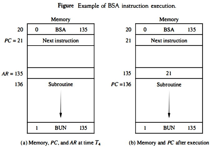
M[AR] ← PC, PC ← AR + 1A numerical example that demonstrates how this instruction is used with a subroutine is shown in Fig. below.
The BSA instruction is assumed to be in memory at address 20. The I bit is 0 and the address part of the instruction has the binary equivalent of 135.
After the fetch and decode phases, PC contains 21, which is the address of the next instruction in the program (referred to as the return address). AR holds the effective address 135.
This is shown in part (a) of the figure. The BSA instruction performs the following numerical operation:
M[135] ← 21, PC ← 135 + 1 = 136The result of this operation is shown in part (b) of the figure. The return address 21 is stored in memory location 135 and control continues with the subroutine program starting from address 136.
The return to the original program (at address 21) is accomplished by means of an indirect BUN instruction placed at the end of the subroutine.
When this instruction is executed, control goes to the indirect phase to read the effective address at location 135, where it finds the previously saved address 21.
When the BUN instruction is executed, the effective address 21 is transferred to PC . The next instruction cycle finds PC with the value 21, so control continues to execute the instruction at the return address.
The BSA instruction performs the function usually referred to as a subroutine call. The indirect BUN instruction at the end of the subroutine performs the function referred to as a subroutine return.
In most commercial computers, the return address associated with a subroutine is stored in either a processor
register or in a portion of memory called a stack. It is not possible to perform the operation of the BSA instruction in one clock cycle when we use the bus system of the basic computer.
To use the memory and the bus properly, the BSA instruction must be executed With a sequence of two microoperations:
D5T4: M[AR] ← PC, AR ← AR + 1
D5T5: PC ← AR, SC ← 0Timing signal T4 initiates a memory write operation, places the content of PC onto the bus, and enables the INR input of AR .
The memory write operation is completed and AR is incremented by the time the next clock transition occurs. The bus is used at T5 to transfer the content of AR to PC .
ISZ: Increment and Skip if Zero
This instruction increments the word specified by the effective address, and if the incremented value is equal to 0, PC is incremented by 1.
The programmer usually stores a negative number (in 2's complement) in the memory word.
As this negative number is repeatedly incremented by one, it eventually reaches the value of zero.
At that time PC is incremented by one in order to skip the next instruction in the program.
Since it is not possible to increment a word inside the memory, it is necessary to read the word into DR, increment DR, and store the word back into memory.
This is done with the following sequence of microoperations:
D6T4: DR ← M [AR]
D6T5: DR ← DR + 1
D6T6: M[AR] ← DR, if (DR = 0) then (PC ← PC + 1), SC ← 0