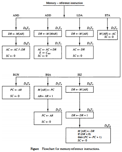
Control Flowchart
A flowchart showing all microoperations for the execution of the seven memory-reference instructions is shown in Fig. below.
The control functions are indicated on top of each box.
The microoperations that are performed during time T4, T5, or T6 depend on the operation code value. This is indicated in the flowchart by six different paths, one of which the control takes after the instruction is decoded.
The sequence counter SC is cleared to 0 with the last timing signal in each case.
This causes a transfer of control to timing signal T0 to start the next instruction cycle.
Note that we need only seven timing signals to execute the longest instruction (ISZ).
The computer can be designed with a 3-bit sequence counter. The reason for using a 4-bit counter for SC is to provide additional timing signals for other instructions that are presented in the problems section.
Input-Output and Interrupt
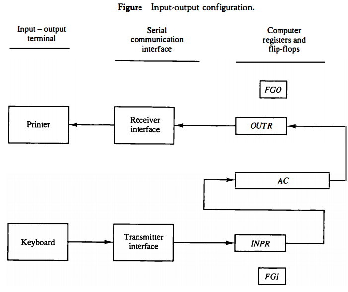
A computer can serve no useful purpose unless it communicates with the external environment. To demonstrate the most basic requirements for input and output communication, we will use as an illustration a terminal unit with a keyboard and printer.
Input-Output Configuration
The terminal sends and receives serial information. Each quantity of information has eight bits of an alphanumeric code.
The serial information from the keyboard is shifted into the input register INPR.
The serial information for the printer is stored in the output register OUTR.
These two registers communicate with a communication interface serially and with the AC in parallel. The input-output configuration is shown in Fig. below. The transmitter interface receives serial information from the keyboard and transmits it to INPR.
The receiver interface receives information from OUTR and sends it to the printer serially.
The input register INPR consists of eight bits and holds an alphanumeric input information. The 1-bit input flag FGI is a control flip-flop. The flag bit is set to 1 when new information is available in the input device and is cleared to 0 when the information is accepted by the computer.
The flag is needed to synchronize the timing rate difference between the input device and the computer.
The process of information transfer is as follows. Initially, the input flag FGI is cleared to 0. When a key is struck in the keyboard, an 8-bit alphanumeric code is shifted into INPR and the input flag FGI is set to 1.
As long as the flag is set, the information in INPR cannot be changed by striking another key. The computer checks the flag bit; if it is 1, the information from INPR is transferred in parallel into AC and FGI is cleared to 0. Once the flag is cleared, new information can be shifted into INPR by striking another key.
The output register OUTR works similarly but the direction of information flow is reversed. Initially, the output flag FGO is set to 1.
The computer checks the flag bit; if it is 1, the information from AC is transferred in parallel to OUTR and FGO is cleared to 0. The output device accepts the coded information, prints the corresponding character, and when the operation is completed, it sets FGO to 1.
The computer does not load a new character into OUTR when FGO is 0 because this condition indicates that the output device is in the process of printing the character.
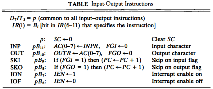
Input-Output Instructions
Input and output instructions are needed for transferring information to and from AC register, for checking the flag bits, and for controlling the interrupt facility.
Input-output instructions have an operation code 1111 and are recognized by the control when D7 = 1 and I = 1. The remaining bits of the instruction specify the particular operation.
The control functions and microoperations for the input-output instructions are listed in Table below. These instructions are executed with the clock transition associated with timing signal T3. Each control function needs a Boolean relation D7IT3, which we designate for convenience by the symbol p. The control function is distinguished by one of the bits in IR(6-11).
By assigning the symbol Bi to bit i of IR, all control functions
can be denoted by pBi for i = 6 though 11. The sequence counter SC is cleared to 0 when p = D7IT3 = 1.The INP instruction transfers the input information from lNPR into the eight low-order bits of AC and also clears the input flag to 0.
The OUT instruction transfers the eight least significant bits of AC into the output register OUTR and clears the output flag to 0.
The next two instructions in Table above check the status of the flags and cause a skip of the next instruction if the flag is 1.
The instruction that is skipped will normally be a branch instruction to return and check the flag again.
The branch instruction is not skipped if the flag is 0. If the flag is 1, the branch instruction is skipped and an input or output instruction is executed.
The last two instructions set and clear an interrupt enable flipflop IEN. The purpose of IEN is explained in conjunction with the interrupt operation
Program Interrupt
The process of communication just described is referred to as programmed control transfer. The computer keeps checking the flag bit, and when it finds it set, it initiates an information transfer.
The difference of information flow rate between the computer and that of the input-output device makes this type of transfer inefficient. To see why this is inefficient, consider a computer that can go through an instruction cycle in 1 μs.
Assume that the input-output device can transfer information at a maximum rate of 10 characters per second. This is equivalent to one character every 100,000 μs. Two instructions are executed when the computer checks the flag bit and decides not to transfer the information.
This means that at the maximum rate, the computer will check the flag 50,000 times between each transfer. The computer is wasting time while checking the flag instead of doing some other useful processing task.
An alternative to the programmed controlled procedure is to let the external device inform the computer when it is ready for the transfer. In the meantime the computer can be busy with other tasks. This type of transfer uses the interrupt facility.
While the computer is running a program, it does not check the flags. However, when a flag is set, the computer is momentarily interrupted from proceeding with the current program and is informed of the fact that a flag has been set.
The computer deviates momentarily from what it is doing to take care of the input or output transfer. It then returns to the current program to continue what it was doing before the interrupt.
The interrupt enable flip-flop IEN can be set and cleared with two instructions. When IEN is cleared to 0 (with the IOF instruction), the flags cannot interrupt the computer. When IEN is set to 1 (with the ION instruction), the computer can be interrupted.
These two instructions provide the programmer with the capability of making a decision as to whether or not to use the interrupt facility.
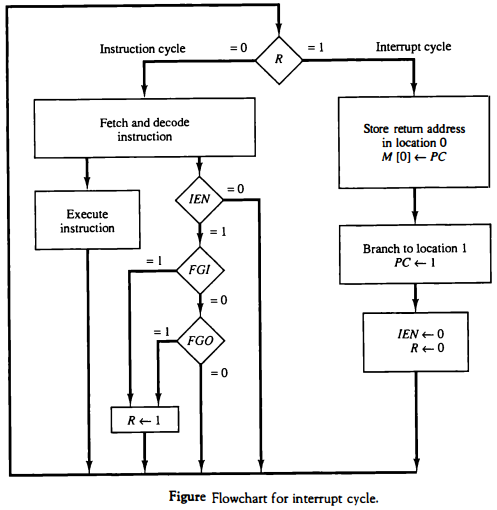
The way that the interrupt is handled by the computer can be explained by means of the flowchart of Fig. above. An interrupt flip-flop R is included in the computer. When R = 0, the computer goes through an instruction cycle.
During the execute phase of the instruction cycle IEN is checked by the control. If it is 0, it indicates that the programmer does not want to use the interrupt, so control continues with the next instruction cycle. If IEN is 1, control checks the flag bits.
If both flags are 0, it indicates that neither the input nor the output registers are ready for transfer of information. In this case, control continues with the next instruction cycle. If either flag is set to 1 while IEN = 1, flip-flop R is set to 1.
At the end of the execute phase, control checks the value of R, and if it is equal to 1, it goes to an interrupt cycle instead of an instruction cycle. The interrupt cycle is a hardware implementation of a branch and save return address operation.
The return address available in PC is stored in a specific location where it can be found later when the program returns to the instruction at which it was interrupted.
This location may be a processor register, a memory stack, or a specific memory location. Here we choose the memory location at address 0 as the place for storing the return address. Control then inserts address 1 into PC and clears IEN and R so that no more interruptions can occur until the interrupt request from the flag has been serviced.
An example that shows what happens during the interrupt cycle is shown in Fig. below. Suppose that an interrupt occurs and R is set to 1 while the control is executing the instruction at address 255. At this time, the return address 256 is in PC .
The programmer has previously placed an input-output service program in memory starting from address 1120 and a BUN 1120 instruction at address 1. This is shown in Part (a) in Fig. below. When control reaches timing signal T0 and finds that R = 1, it proceeds with the interrupt cycle.
The content of PC (256) is stored in memory location 0, PC is set to 1, and R is cleared to 0. At the beginning of the next instruction cycle, the instruction that is read from memory is in address 1 since this is the content of PC.
The branch instruction at address 1 causes the program to transfer to the input-output service program at address 1120. This program checks the flags, determines which flag is set, and then transfers the required input or output information.
Once this is done, the instruction ION is executed to set IEN to 1 (to enable further interrupts), and the program returns to the location where it was interrupted. This is shown in Part (b) in Fig. below.
The instruction that returns the computer to the original place in the main program is a branch indirect instruction with an address part of 0. This instruction is placed at the end of the UO service program.
After this instruction is
read from memory during the fetch phase, control goes to the indirect phase (because I = 1) to read the effective address.The effective address is in location 0 and is the return address that was stored there during the previous interrupt cycle. The execution of the indirect BUN instruction results in placing into PC the return address from location 0.
Interrupt Cycle
The interrupt cycle is initiated after the last execute phase if the interrupt flip-flop R is equal to 1. This flip-flop is set to 1 if IEN = 1 and either FGI or FGO are equal to 1.
This can happen with any clock transition except when timing signals T0, T1 or T2 are active. The condition for setting flip-flop R to 1 can be expressed with the following register transfer statement: \( T_0'T_1'T_2'(IEN)(FGI+FGO): R \leftarrow 1 \)
The symbol + between FGI and FGO in the control function designates a logic OR operation. This is ANDed with IEN and \( T_0'T_1'T_2' \).
We now modify the fetch and decode phases of the instruction cycle. Instead of using only timing signals T0, T1 or T2 (as shown in Figure in Section - Determine the Type of Instruction) we will AND the three timing signals with R' so that the fetch and decode phases will be recognized from the three control functions R'T0, R'T1 and R'T2.
The reason for this is that after the instruction is executed and SC is cleared to 0, the control will go through a fetch phase only if R = 0. Otherwise, if R = 1, the control will go through an interrupt cycle.
The interrupt cycle stores the return address (available in PC) into memory location 0, branches to memory location 1, and clears IEN, R, and SC to 0. This can be done with the following sequence of microoperations:
RT0: AR ← 0, TR ← PC
RT1: M[AR] ← TR, PC ← 0
RT2: PC ← PC + 1, IEN ← 0, R ← 0, SC ← 0
During the first timing signal AR is cleared to 0, and the content of PC is transferred to the temporary register TR.
With the second timing signal, the return address is stored in memory at location 0 and PC is cleared to 0. The third timing signal increments PC to 1, clears IEN and R, and control goes back to T0 by clearing SC to 0.
The beginning of the next instruction cycle has the condition R'T0 and the content of PC is equal to 1.
The control then goes through an instruction cycle that fetches and executes the BUN instruction in location 1.