Central Processing Unit - Introduction
The part of the computer that performs the bulk of data-processing operations is called the central processing unit and is referred to as the CPU.
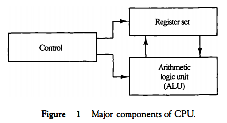
The CPU is made up of three major parts, as shown in Fig. 1. The register set stores intermediate data used during the execution of the instructions. The arithmetic logic unit (ALU) performs the required microoperations for executing the instructions. The control unit supervises the transfer of information among the registers and instructs the ALU as to which operation to perform.
The CPU performs a variety of functions dictated by the type of instructions that are incorporated in the computer.
Computer architecture is sometimes defined as the computer structure and behavior as seen by the programmer that uses machine language instructions.
This includes the instruction formats, addressing modes, the instruction set, and the general organization of the CPU registers.
One boundary where the computer designer and the computer programmer see the same machine is the part of the CPU associated with the instruction set.
From the designer's point of view, the computer instruction set provides the specifications for the design of the CPU.
The design of a CPU is a task that in large part involves choosing the hardware for implementing the machine instructions.
The user who programs the computer in machine or assembly language must be aware of the register set, the memory structure, the type of data supported by the instructions, and the function that each instruction performs.
General Register Organization
Memory locations are needed for storing pointers, counters, return addresses, temporary results, and partial products during multiplication.
Having to refer to memory locations for such applications is time consuming because memory access is the most time-consuming, operation in a computer.
It is more convenient and more efficient to store these intermediate values in processor registers.
When a large number of registers are included in the CPU, it is most efficient to connect them through a common bus system. The registers communicate with each other not only for direct data transfers, but also while performing various microoperations.
Hence it is necessary to provide a common unit that can perform all the arithmetic, logic, and shift microoperations in the processor.
A bus organization for seven CPU registers is shown in Fig. 2. The output of each register is connected to two multiplexers (MUX) to form the two buses A and B. The selection lines in each multiplexer select one register or the input data for the particular bus.
The A and B buses form the inputs to a common arithmetic logic unit (ALU).
The operation selected in the ALU determines the arithmetic or logic micro-operation that is to be performed.
The result of the microoperation is available for output data and also goes into the inputs of all the registers.
The register that receives the information from the output bus is selected by a decoder.
The decoder activates one of the register load inputs, thus providing a transfer path between the data in the output bus and the inputs of the selected destination register.
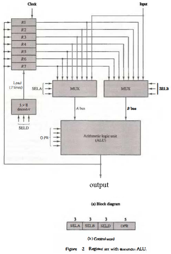
The control unit that operates the CPU bus system directs the information flow through the registers and ALU by selecting the various components in the system. For example, to perform the operation R1 ← R2 + R3
the control must provide binary selection variables to the following selector inputs:
MUX A selector (SELA): to place the content of R2 into bus A.
MUX B selector (SELB): to place the content o f R 3 into bus B.
ALU operation selector (OPR): to provide the arithmetic addition A + B.
Decoder destination selector (SELD): to transfer the content of the output bus into R1.
The four control selection variables are generated in the control unit and must be available at the beginning of a clock cycle.
The data from the two source registers propagate through the gates in the multiplexers and the ALU, to the output bus, and into the inputs of the destination register, all during the clock cycle interval.
Then, when the next clock transition occurs, the binary information from the output bus is transferred into R1.
To achieve a fast response time, the ALU is constructed with high-speed circuits.
Control Word
There are 14 binary selection inputs in the unit, and their combined value specifies a control word. The 14-bit control word is defined in Fig. 2(b).
It consists of four fields. Three fields contain three bits each, and one field has five bits.
The three bits of SELA select a source register for the A input of the ALU. The three bits of SELB select a register for the B input of the ALU.
The three bits of SELD select a destination register using the decoder and its seven load outputs.
The five bits of OPR select one of the operations in the ALU.
The 14-bit control word when applied to the selection inputs specify a particular microoperation.
The encoding of the register selections is specified in Table 1.
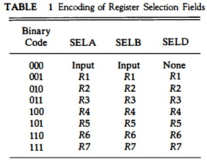
The 3-bit binary code listed in the first column of the table specifies the binary code for each of the three fields.
The register selected by fields SELA, SELB, and SELD is the one whose decimal number is equivalent to the binary number in the code. When SELA or SELB is 000, the corresponding multiplexer selects the external input data.
When SELD = 000, no destination register is selected but the contents of the output bus are available in the external output. The ALU provides arithmetic and logic operations.
In addition, the CPU must provide shift operations. The shifter may be placed in the input of the ALU to provide a preshift capability, or at the output of the ALU to provide postshifting capability. In some cases, the shift operations are included with the ALU.
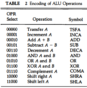
The function table for this ALU is listed in Table 8. The encoding of the ALU operations for the CPU is specified in Table 2. The OPR field has five bits and each operation is designated with a symbolic name.
Examples of Microoperations
A control word of 14 bits is needed to specify a microoperation in the CPU. The control word for a given microoperation can be derived from the selection variables.
For example, the subtract rnicrooperation given by the statement R1 ← R2 - R3 specifies R2 for the A input of the ALU, R3 for the B input of the ALU, R1 for the destination register, and an ALU operation to subtract A - B.
Thus the control word is specified by the four fields and the corresponding binary value for each field is obtained from the encoding listed in Tables 1 and 2.
The binary control word for the subtract rnicrooperation is 010 011 001 00101 and is obtained as follows:
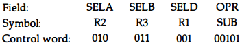
The control word for this rnicrooperation and a few others are listed in Table 3.
The increment and transfer microoperations do not use the B input of the ALU.
For these cases, the B field is marked with a dash. We assign 000 to any unused field when formulating the binary control word, although any other binary number may be used.
To place the content of a register into the output terminals we place the content of the register into the A input of the ALU, but none of the registers are selected to accept the data.
The ALU operation TSFA places the data from the register, through the ALU, into the output terminals.
The direct transfer from input to output is accomplished with a control word
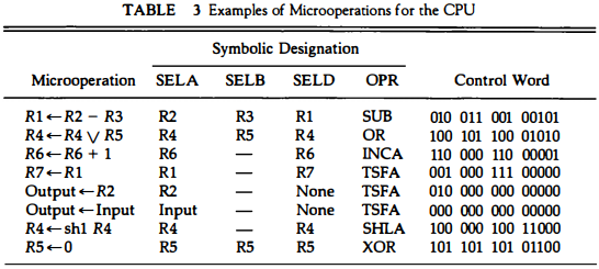
of all 0's (making the B field 000).
A register can be cleared to 0 with an exclusive-OR operation. This is because x ⊕ x = 0.
It is apparent from these examples that many other microoperations can be generated in the CPU.
The most efficient way to generate control words with a large number of bits is to store them in a memory unit.
A memory unit that stores control words is referred to as a control memory.
By reading consecutive control words from memory, it is possible to initiate the desired sequence of microoperations for the CPU.
This type of control is referred to as microprogrammed control.