Data Dependency
A difficulty that may caused a degradation of performance in an instruction pipeline is due to possible collision of data or address.
A collision occurs when an instruction cannot proceed because previous instructions did not complete certain operations.
A data dependency occurs when an instruction needs data that are not yet available.
For example, an instruction in the FO segment may need to fetch an operand that is being generated at the same time by the previous instruction in segment EX.
Therefore, the second instruction must wait for data to become available by the first instruction. Similarly, an address dependency may occur when an operand address cannot be calculated because the information needed by the addressing mode is not available.
For example, an instruction with register indirect mode cannot proceed to fetch the operand if the previous instruction is loading the address into the register.
Therefore, the operand access to memory must be delayed until the required address is available. Pipelined computers deal with such conflicts between data dependencies in a variety of ways.
The most straightforward method is to insert hardware interlocks. An interlock is a circuit that detects instructions whose source operands are destinations of instructions farther up in the pipeline.
Detection of this situation causes the instruction whose source is not available to be delayed by enough clock cycles to resolve the conflict. This approach maintains the program sequence by using hardware to insert the required delays.
Another technique called operand forwarding uses special hardware to detect a conflict and then avoid it by routing the data through special paths between pipeline segments.
For example, instead of transferring an ALU result into a destination register, the hardware checks the destination operand, and if it is needed as a source in the next instruction, it passes the result directly into the ALU input, bypassing the register.
This method requires additional hardware paths through multiplexers as well as the circuit that detects the conflict.
A procedure employed in some computers is to give the responsibility for solving data conflicts problems to the compiler that translates the high-level programming language into a machine language program.
The compiler for such computers is designed to detect a data conflict and reorder the instructions as necessary to delay the loading of the conflicting data by inserting no-operation instructions. This method is referred to as delayed load.
Handling of Branch Instructions
One of the major problems in operating an instruction pipeline is the occurrence of branch instructions.
A branch instruction can be conditional or unconditional. An unconditional branch always alters the sequential program flow by loading the program counter with the target address.
In a conditional branch, the control selects the target instruction if the condition is satisfied or the next sequential instruction if the condition is not satisfied. As mentioned previously, the branch instruction breaks the norrnal sequence of the instruction stream, causing difficulties in the operation of the instruction pipeline.
Pipelined computers employ various hardware techniques to minimize the performance degradation caused by instruction branching. One way of handling a conditional branch is to prefetch the target instruction in addition to the instruction following the branch. Both are saved until the branch is executed. If the branch condition is successful, the pipeline continues from the branch target instruction. An extension of this procedure is to continue fetching instructions from both places until the branch decision is made. At that time control chooses the instruction stream of the correct program flow.
Another possibility is the use of a branch target buffer or BTB.
The BTB is an associative memory included in the fetch segment of the pipeline. Each entry in the BTB consists of the address of a previously executed branch instruction and the target instruction for that branch.
It also stores the next few instructions after the branch target instruction. When the pipeline decodes a branch instruction, it searches the associative memory BTB for the address of the instruction.
If it is in the BTB, the instruction is available directly and prefetch continues from the new path.
If the instruction is not in the BTB, the pipeline shifts to a new instruction stream and stores the target instruction in the BTB. The advantage of this scheme is that branch instructions that have occurred previously are readily available in the pipeline without interruption. A variation of the BTB is the loop buffer.
This is a small very high speed register file maintained by the instruction fetch segment of the pipeline. When a program loop is detected in the program, it is stored in the loop buffer in its entirety, including all branches.
The program loop can be executed directly without having to access memory until the loop mode is removed by the final branching out. Another procedure that some computers use is branch prediction . A pipeline with branch prediction uses some additional logic to guess the outcome of a conditional branch instruction before it is executed.
The pipeline then begins prefetching the instruction stream from the predicted path. A correct prediction eliminates the wasted time caused by branch penalties. A procedure employed in most ruse processors is the delayed branch .
In this procedure, the compiler detects the branch instructions and rearranges the machine language code sequence by inserting useful instructions that keep the pipeline operating without interruptions.
An example of delayed branch is the insertion of a no-operation instruction after a branch instruction. This causes the computer to fetch the target instruction during the execution of the no operation instruction, allowing a continuous flow of the pipeline.
RISC Pipeline
Among the characteristics attributed to ruse is its ability to use an efficient instruction pipeline.
The simplicity of the instruction set can be utilized to implement an instruction pipeline using a small number of suboperations, with each being executed in one clock cycle.
Because of the fixed-length instruction format, the decoding of the operation can occur at the same time as the register selection. All data manipulation instructions have register-toregister operations.
Since all operands are in registers, there is no need for calculating an effective address or fetching of operands from memory. Therefore, the instruction pipeline can be implemented with two or three segments. One segment fetches the instruction from program memory, and the other segment executes the instruction in the ALU.
A third segment may be used to store the result of the ALU operation in a destination register. The data transfer instructions in RISC are limited to load and store instructions. These instructions use register indirect addressing.
They usually need three or four stages in the pipeline. To prevent conflicts between a memory access to fetch an instruction and to load or store an operand, most RISC machines use two separate buses with two memories: one for storing the instructions and the other for storing the data. The two memories can sometime operate at the same speed as the CPU clock and are referred to as cache memories.
One of the major advantages of RISC is its ability to execute instructions at the rate of one per clock cycle. It is not possible to expect that every instruction be fetched from memory and executed in one clock cycle.
What is done, in effect, is to start each instruction with each clock cycle and to pipeline the processor to achieve the goal of single-cycle instruction execution.
The advantage of RISC over OSC (complex instruction set computer) is that RISC can achieve pipeline segments, requiring just one clock cycle, while OSC uses many segments in its pipeline, with the longest segment requiring two or more clock cycles. Another characteristic of RISC is the support given by the compiler that translates the high-level language program into machine language program.
Instead of designing hardware to handle the difficulties associated with data conflicts and branch penalties, RISC processors rely on the efficiency of the compiler to detect and minimize the delays encountered with these problems.
Example: Three-Segment Instruction Pipeline
The data manipulation instructions operate on data in processor registers. The data transfer instructions are load and store instructions that use an effective address obtained from the addition of the contents of two registers or a register and a displacement constant provided in the instruction.
The program control instructions use register values and a constant to evaluate the branch address, which is transferred to a register or the program counter PC.
Now consider the hardware operation for such a computer. The control section fetches the instruction from program memory into an instruction register. The instruction is decoded at the same time that the registers needed for the execution of the instruction are selected.
The processor unit consists of a number of registers and an arithmetic logic unit (ALU) that performs the necessary arithmetic, logic, and shift operations. A data memory is used to load or store the data from a selected register in the register file. The instruction cycle can be divided into three suboperations and implemented in three segments:
I: Instruction fetch
A: ALU operation
E: Execute instruction
The I segment fetches the instruction from program memory. The instruction is decoded and an ALU operation is performed in the A segment.
The ALU is used for three different functions, depending on the decoded instruction. It performs an operation for a data manipulation instruction, it evaluates the effective address for a load or store instruction, or it calculates the branch address for a program control instruction.
The E segment directs the output of the ALU to one of three destinations, depending on the decoded instruction. It transfers the result of the ALU operation into a destination register in the register file, it transfers the effective address to a data memory for loading or storing, or it transfers the branch address to the program counter.
Delayed Load
Consider now the operation of the following four instructions:
1. LOAD: R1 ← M [address 1]
2. LOAD: R2 ← M [address 2]
3. ADD: R3 ← R1 + R2
4. STORE: M[address 3] ← R3
If the three-segment pipeline proceeds without interruptions, there will be a data conflict in instruction 3 because the operand in R2 is not yet available in the A segment.
This can be seen from the timing of the pipeline shown in Fig. 9(a). The E segment in clock cycle 4 is in a process of placing the memory data into R2.
The A segment in clock cycle 4 is using the data from R2, but the value in R2 will not be the correct value since it has not yet been transferred from memory.
It is up to the compiler to make sure that the instruction following the load instruction uses the data fetched from memory. If the compiler cannot find a useful instruction to put after the load, it inserts a no-op (no-operation) instruction.
This is a type of instruction that is fetched from
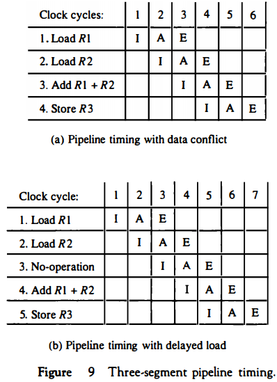
memory but has no operation, thus wasting a clock cycle. This concept of delaying the use of the data loaded from memory is referred to as delayed load.
Figure 9(b) shows the same program with a no-op instruction inserted after the load to R2 instruction. The data is loaded into R2 in clock cycle 4.
The add instruction uses the value of R2 in step 5.
Thus the no-op instruction is used to advance one clock cycle in order to compensate for the data conflict in the pipeline. (Note that no operation is performed in segment A during clock cycle 4 or segment E during clock cycle 5.)
The advantage of the delayed load approach is that the data dependency is taken care of by the compiler rather than the hardware.
This results in a simpler hardware segment since the segment does not have to check if the content of the register being accessed is currently valid or not.
Input-Output Interface
Input-output interface provides a method for transferring information between internal storage and external I/O devices.
Peripherals connected to a computer need special communication links for interfacing them with the central processing unit.
The purpose of the communication link is to resolve the differences that exist between the central computer and each peripheral.
The major differences are:
1. Peripherals are electromechanical and electromagnetic devices and their
manner of operation is different from the operation of the CPU and
memory, which are electronic devices. Therefore, a conversion of signal
values may be required.

2. The data transfer rate of peripherals is usually slower than the transfer
rate of the CPU, and consequently, a synchronization mechariism may
be needed.

3. Data codes and formats in peripherals differ from the word format in
the CPU and memory.

4. The operating modes of peripherals are different from each other and
each must be controlled so as not to disturb the operation of other
peripherals connected to the CPU.
To resolve these differences, computer systems include special hardware components between the CPU and peripherals to supervise and synchronize all input and output transfers. These components are called interface units because they interface between the processor bus and the peripheral device.
In addition, each device may have its own controller that supervises the operations of the particular mechanism in the peripheral.
I/O Bus and Interface Modules
A typical communication link between the processor and several peripherals is shown in Fig. 1.
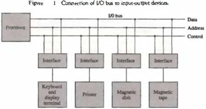
The I/O bus consists of data lines, address lines, and control lines.
The magnetic disk, printer, and terminal are employed in any general-purpose computer. The magnetic tape is used in some computers for backup storage.
Each peripheral device has associated with it an interface unit. Each interface decodes the address and control received from the I/O bus, interprets them for the peripheral, and provides signals for the peripheral controller.
It also synchronizes the data flow and supervises the transfer between peripheral and processor. Each peripheral has its own controller that operates the particular electromechanical device.
For example, the printer controller controls the paper motion, the print timing, and the selection of printing characters.
A controller may be housed separately or may be physically integrated with the peripheral.
The I/O bus from the processor is attached to all peripheral interfaces. To communicate with a particular device, the processor places a device address on the address lines. Each interface attached to the I/O bus contains an address decoder that monitors the address lines.
When the interface detects its own address, it activates the path between the bus lines and the device that it controls. All peripherals whose address does not correspond to the address in the bus are disabled by their interface.
At the same time that the address is made available In the address lines, the processor provides a function code in the control lines.
The interface selected responds to the function code and proceeds to execute it.
The function code is referred to as an I/O command and is in essence an instruction that is executed in the interface and its attached peripheral unit. The interpretation of the command depends on the peripheral that the processor is addressing.
There are four types of commands that an interface may receive. They are classified as control, status, data output, and data input.
A control command is issued to activate the peripheral and to inform it what to do. For example, a magnetic tape unit may be instructed to backspace the tape by one record, to rewind the tape, or to start the tape moving in the forward direction.
The particular control command issued depends on the peripheral, and each peripheral receives its own distinguished sequence of control commands, depending on its mode of operation.
A status command is used to test various status conditions in the interface and the peripheral. For example, the computer may wish to check the status of the peripheral before a transfer is initiated. During the transfer, one or more errors may occur which are detected by the interface.
These errors are designated by setting bits in a status register that the processor can read at certain intervals.
A data output command causes the interface to respond by transferring data from the bus into one of its registers. Consider an example with a tape unit.
The computer starts the tape moving by issuing a control command. The processor then monitors the status of the tape by means of a status command.
When the tape is in the correct position, the processor issues a data output command. The interface responds to the address and command and transfers the information from the data lines in the bus to its buffer register. The interface then communicates with the tape controller and sends the data to be stored on tape.
The data input command is the opposite of the data output. In this case the interface receives an item of data from the peripheral and places it in its buffer register.
The processor checks if data are available by means of a status command and then issues a data input command. The interface places the data on the data lines, where they are accepted by the processor.
I/O versus Memory Bus
In addition to communicating with I/O, the processor must communicate with the memory unit. Like the I/O bus, the memory bus contains data, address, and read/write control lines. There are three ways that computer buses can be used to communicate with memory and I/O:
Use two separate buses, one for memory and the other for I/O.
Use one common bus for both memory and I/O but have separate control lines for each.
Use one common bus for memory and I/O with common control lines.
In the first method, the computer has independent sets of data, address, and control buses, one for accessing memory and the other for I/O.
This is done IOP in computers that provide a separate I/O processor (IOP) in addition to the central processing unit (CPU).
The memory communicates with both the CPU and the IOP through a memory bus.
The IOP communicates also with the input and output devices through a separate I/O bus with its own address, data and control lines.
The purpose of the IOP is to provide an independent pathway for the transfer of information between external devices and internal memory. The I/O processor is sometimes called a data channel.
Isolated versus Memory-Mapped I/O
Many computers use one common bus to transfer information between memory or I/O and the CPU.
The distinction between a memory transfer and I/O transfer is made through separate read and write lines. The CPU specifies whether the address on the address lines is for a memory word or for an interface register by enabling one of two possible read or write lines.
The I/O read and I/O write control lines are enabled during an I/O transfer. The memory read and memory write control lines are enabled during a memory transfer.
This configuration isolates all I/O interface addresses from the addresses assigned to memory and is referred to as the isolated I/O method for assigning addresses in a common bus.
In the isolated I/O configuration, the CPU has distinct input and output instructions, and each of these instructions is associated with the address of an interface register.
When the CPU fetches and decodes the operation code of an input or output instruction, it places the address associated with the instruction into the common address lines.
At the same time, it enables the I/O read (for input) or I/O write (for output) control line. This informs the external components that are attached to the common bus that the address in the address lines is for an interface register and not for a memory word.
On the other hand, when the CPU is fetching an instruction or an operand from memory, it places the memory address on the address lines and enables the memory read or memory write control line.
This informs the external components that the address is for a memory word and not for an I/O interface.
The isolated I/O method isolates memory and I/O addresses so that memory address values are not affected by interface address assignment since each has its own address space.
The other alternative is to use the same address space for both memory and I/O.
This is the case in computers that employ only one set of read and write signals and do not distinguish between memory and I/O addresses.
This configuration is referred to as memory-mapped I/O. The computer treats an interface register as being part of the memory system.
The assigned addresses for interface registers cannot be used for memory words, which reduces the memory address range available.
In a memory-mapped I/O organization there are no specific input or output instructions.
The CPU can manipulate I/O data residing in interface registers with the same instructions that are used to manipulate memory words.
Each interface is organized as a set of registers that respond to read and write requests in the normal address space.
Typically, a segment of the total address space is reserved for interface registers, but in general, they can be located at any address as long as there is not also a memory word that responds to the same address.
Computers with memory-mapped I/O can use memory-type instructions to access I/O data.
It allows the computer to use the same instructions for either input-output transfers or for memory transfers.
The advantage is that the load and store instructions used for reading and writing from memory can be used to input and output data from I/O registers.
In a typical computer, there are more memory-reference instructions than I/O instructions. With memory mapped I/O all instructions that refer to memory are also available for I/O.
Example of I/O Interface
An example of an I/O interface unit is shown in block diagram form in Fig. 2.
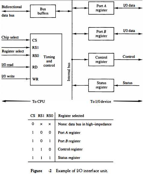
It consists of two data registers called ports, a control register, a status register, bus buffers, and timing and control circuits.
The interface communicates with the CPU through the data bus. The chip select and register select inputs determine the address assigned to the interface.
The I/O read and write are two control lines that specify an input or output, respectively. The four registers communicate directly with the I/O device attached to the interface.
The I/O data to and from the device can be transferred into either port A or port B. The interface may operate with an output device or with an input device, or with a device that requires both input and output.
If the interface is connected to a printer, it will only output data, and if it services a character reader, it will only input data.
A magnetic disk unit transfers data in both directions but not at the same time, so the interface can use bidirectional lines.
A command is passed to the I/O device by sending a word to the appropriate interface register.
In a system like this, the function code in the I/O bus is not needed because control is sent to the control register, status information is received from the status register, and data are transferred to and from ports A and B registers.
Thus the transfer of data, control, and status information is always via the common data bus.
The distinction between data, control, or status information is determined from the particular interface register with which the CPU communicates.
The control register receives control information from the CPU. By loading appropriate bits into the control register, the interface and the I/O device attached to it can be placed in a variety of operating modes.
For example, port A may be defined as an input port and port B as an output port.
A magnetic tape unit may be instructed to rewind the tape or to start the tape moving in the forward direction.
The bits in the status register are used for status conditions and for recording errors that may occur during the data transfer.
For example, a status bit may indicate that portA has received a new data item from the I/O device.
Another bit in the status register may indicate that a parity error has occurred during the transfer.
The interface registers communicate with the CPU through the bidirectional data bus.
The address bus selects the interface unit through the chip select and the two register select inputs.
A circuit must be provided externally (usually, a decoder) to detect the address assigned to the interface registers.
This circuit enables the chip select (CS) input when the interface is selected by the address bus. The two register select inputs RS1 and RS0 are usually connected to the two least significant lines of the address bus.
These two inputs select one of the four registers in the interface as specified in the table accompanying the diagram.
The content of the selected register is transfer into the CPU via the data bus when the I/O read signal is enabled.
The CPU transfers binary information into the selected register via the data bus when the I/O write input is enabled.