Memory Organization
The memory unit is an essential component in any digital computer since it is needed for storing programs and data.
A very small computer with a limited application may be able to fulfill its intended task without the need for additional storage capacity.
Most general purpose computers would run more efficiently if they were equipped with additional storage beyond the capacity of the main memory.
There is just not enough space in one memory unit to accommodate all the programs used in a typical computer.
Moreover, most computer users accumulate and continue to accumulate large amounts of data-processing software.
Not all accumulated information is needed by the processor at the same time.
Therefore, it is more economical to use low-cost storage devices to serve as a backup for storing the information that is not currently used by the CPU.
The memory unit that communicates directly with the CPU is called the main memory.
Devices that provide backup storage are auxiliary memory.
The most common auxiliary memory devices used in computer systems are magnetic disks and tapes.
They are used for storing system programs, large data files, and other backup information.
Only programs and data currently needed by the processor reside in main memory.
All other information is stored in auxiliary memory and transferred to main memory when needed.
The total memory capacity of a computer can be visualized as being a hierarchy of components.
The memory hierarchy system consists of all storage devices employed in a computer system from the slow but high-capacity auxiliary memory to a relatively faster main memory, to an even smaller and faster cache memory accessible to the high-speed processing logic.
Figure 1 illustrates the components in a typical memory hierarchy. At the bottom of the hierarchy are the relatively slow magnetic tapes used to store removable files.
Next are the magnetic disks used as backup storage. The main memory occupies a central position by being able to communicate directly with the CPU and with auxiliary memory devices through an I/O processor.
When programs not residing in main memory are needed by the CPU, they are brought in from auxiliary memory.
Programs not currently needed in main memory are transferred into auxiliary memory to provide space for currently used programs and data.
A special very-high speed memory called a cache is sometimes used to increase the speed of processing by making current programs and data available to the CPU at a rapid rate.
The cache memory is employed in computer systems to compensate for the speed differential between main memory access time and processor logic.
CPU logic is usually faster than main memory access time, with the result that processing speed is limited primarily by the speed of main memory.
A technique used to compensate for the mismatch in operating speeds is to employ an extremely fast, small cache between the CPU and main memory whose access time is close to processor logic clock cycle time.
The cache is used for storing segments of programs currently being executed in the CPU and temporary data frequently needed in the present calculations.
By making programs and data available at a rapid rate, it is possible to increase the performance rate of the computer.
While the I/O processor manages data transfers between auxiliary memory and main memory, the cache organization is concerned with the transfer of information between main memory and CPU.
Thus each is involved with a different level in the memory hierarchy system.
The reason for having two or three levels of memory hierarchy is economics.
As the storage capacity of the memory increases, the cost per bit for storing binary information decreases and the access time of the memory becomes longer.
The auxiliary memory has a large storage capacity, is relatively inexpensive, but has low access speed compared to main memory.
The cache memory is very small, relatively expensive, and has very high access speed. Thus as the memory access speed increases, so does its relative cost.
The overall goal of using a memory hierarchy is to obtain the highest-possible average access speed while minimizing the total cost of the entire memory system.
Auxiliary and cache memories are used for different purposes. The cache holds those parts of the program and data that are most heavily used, while the auxiliary memory holds those parts that are not presently used by the CPU.
Moreover, the CPU has direct access to both cache and main memory but not to auxiliary memory. The transfer from auxiliary to main memory is usually done by means of direct memory access of large blocks of data.
The typical access time ratio between cache and main memory is about 1 to 7. For example, a typical cache memory may have an access time of 100 ns, while main memory access time may be 700 ns.
Auxiliary memory average access time is usually 1000 times that of main memory. Block size in auxiliary memory typically ranges from 256 to 2048 words, while cache block size is typically from 1 to 16 words.
Many operating systems are designed to enable the CPU to process a number of independent programs concurrently.
This concept, called multiprogramming, refers to the existence of two or more programs in different parts of the memory hierarchy at the same time.
In this way it is possible to keep all parts of the computer busy by working with several programs in sequence. For example, suppose that a program is being executed in the CPU and an VO transfer is required.
The CPU initiates the I/O processor to start executing the transfer. This leaves the CPU free to execute another program. In a multiprogramming system, when one program is waiting for input or output transfer, there is another program ready to utilize the CPU.
With multiprogramming the need arises for running partial programs, for varying the amount of main memory in use by a given program, and for moving programs around the memory hierarchy.
Computer programs are sometimes too long to be accommodated in the total space available in main memory.
Moreover, a computer system uses many programs and all the programs cannot reside in main memory at all times. A program with its data normally resides in auxiliary memory.
When the program or a segment of the program is to be executed, it is transferred to main memory to be executed by the CPU. Thus one may think of auxiliary memory as containing the totality of information stored in a computer system.
It is the task of the operating system to maintain in main memory a portion of this information that is currently active.
The part of the computer system that supervises the flow of information between auxiliary memory and main memory is called the memory management system.
Main Memory
The main memory is the central storage unit in a computer system. It is a relatively large and fast memory used to store programs and data during the computer operation.
The principal technology used for the main memory is based on semiconductor integrated circuits.
Integrated circuit RAM chips are available in two possible operating modes, static and dynamic. The static RAM consists essentially of internal flip-flops that store the binary information.
The stored information remains valid as long as power is applied to the unit. The dynamic RAM stores the binary information in the form of electric charges that are applied to capacitors.
The capacitors are provided inside the chip by MOS transistors.
The stored charge on the capacitors tend to discharge with time and the capacitors must be periodically recharged by refreshing the dynamic memory.
Refreshing is done by cycling through the words every few milliseconds to restore the decaying charge. The dynamic RAM offers reduced power consumption and larger storage capacity in a single memory chip.
The static RAM is easier to use and has shorter read and write cycles. Most of the main memory in a general-purpose computer is made up of RAM integrated circuit chips, but a portion of the memory may be constructed with ROM chips.
Originally, RAM was used to refer to a random-access memory, but now it is used to designate a read/write memory to distinguish it from a read-only memory, although ROM is also random access.
RAM is used for storing the bulk of the programs and data that are subject to change.
ROM is used for storing programs that are permanently resident in the computer and for tables of constants that do not change in value once the production of the computer is completed.
Among other things, the ROM portion of main memory is needed for storing an initial program called a bootstrap loader.
The bootstrap loader is a program whose function is to start the computer software operating when power is turned on.
Since RAM is volatile, its contents are destroyed when power is turned off.
The contents of ROM remain unchanged after power is turned off and on again.
The startup of a computer consists of turning the power on and starting the execution of an initial program.
Thus when power is turned on, the hardware of the computer sets the program counter to the first address of the bootstrap loader.
The bootstrap program loads a portion of the operating system from disk to main memory and control is then transferred to the operating system, which prepares the computer for general use.
RAM and ROM chips are available in a variety of sizes. If the memory needed for the computer is larger than the capacity of one chip, it is necessary to combine a number of chips to form the required memory size.
To demonstrate the chip interconnection, we will show an example of a 1024 x 8 memory constructed with 128 x 8 RAM chips and 512 x 8 ROM chips.
RAM and ROM Chips
A RAM chip is better suited for communication with the CPU if it has one or more control inputs that select the chip only when needed.
Another common feature is a bidirectional data bus that allows the transfer of data either from memory to CPU during a read operation, or from CPU to memory during a write operation.
A bidirectional bus can be constructed with three-state buffers. A three-state buffer output can be placed in one of three possible states: a signal equivalent to logic 1, a signal equivalent to logic 0, or a highimpedance state.
The logic 1 and 0 are normal digital signals. The high impedance state behaves like an open circuit, which means that the output does not carry a signal and has no logic significance.
The block diagram of a RAM chip is shown in Fig. 2. The capacity of the memory is 128 words of eight bits (one byte) per word. This requires a 7-bit
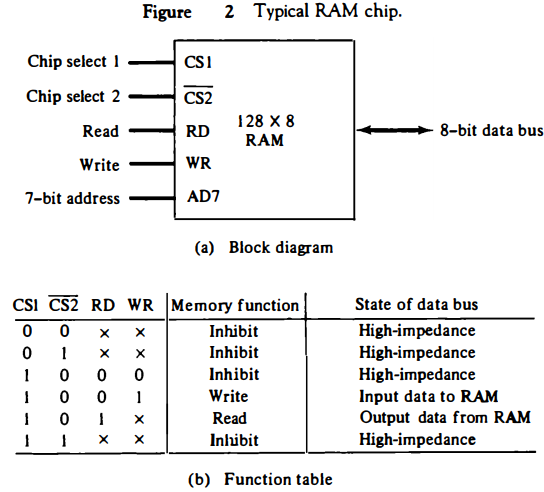 address and an 8-bit bidirectional data bus.
The read and write inputs specifies the memory operation and the two chips select (CS) control inputs are for enabling the chip only when it is selected by the microprocessor.
The availability of more than one control input to select the chip facilitates the decoding of the address lines when multiple chips are used in the microcomputer.
The read and write inputs are sometimes combined into one line labeled R/W. When the chip is selected, the two binary states in this line specify the two operations of read or write.
The function table listed in Fig. 2(b) specifies the operation of the RAM chip. The unit is in operation only when CS1 = 1 and CS2 = 0. The bar on top of the second select variable indicates that this input is enabled when it is equal to 0.
If the chip select inputs are not enabled, or if they are enabled but the read or write inputs are not enabled, the memory is inhibited and its data bus is in a high-impedance state.
When CS1 = 1 and CS2 = 0, the memory can be placed in a write or read mode.
When the WR input is enabled, the memory stores a byte from the data bus into a location specified by the address input lines.
When the RD input is enabled, the content of the selected byte is placed into the data bus. The RD and WR signals control the memory operation as well as the bus buffers associated with the bidirectional data bus .
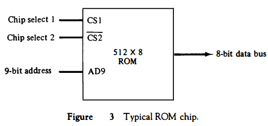
A ROM chip is organized externally in a similar manner. However, since a ROM can only read, the data bus can only be in an output mode. The block diagram of a ROM chip is shown in Fig. 3. For the same-size chip, it is possible to have more bits of ROM than of RAM, because the internal binary cells in ROM occupy less space than in RAM.
For this reason, the diagram specifies a 512-byte ROM, while the RAM has only 128 bytes.
The nine address lines in the ROM chip specify any one of the 512 bytes stored in it.
The two chip select inputs must be CS1 = 1 and CS2 = 0 for the unit to operate. Otherwise, the data bus is in a high-impedance state.
There is no need for a read or write control because the unit can only read. Thus when the chip is enabled by the two select inputs, the byte selected by the address lines appears on the data bus.
Memory Address Map
The designer of a computer system must calculate the amount of memory required for the particular application and assign it to either RAM or ROM.
The interconnection between memory and processor is then established from knowledge of the size of memory needed and the type of RAM and ROM chips available.
The addressing of memory can be established by means of a table that specifies the memory address assigned to each chip.
The table, called a memory address map, is a pictorial representation of assigned address space for each chip in the system.
To demonstrate with a particular example, assume that a computer system needs 512 bytes of RAM and 512 bytes of ROM. The RAM and ROM chips to be used are specified in Figs. 2 and 3.
The memory address map for this configuration is shown in Table 1.
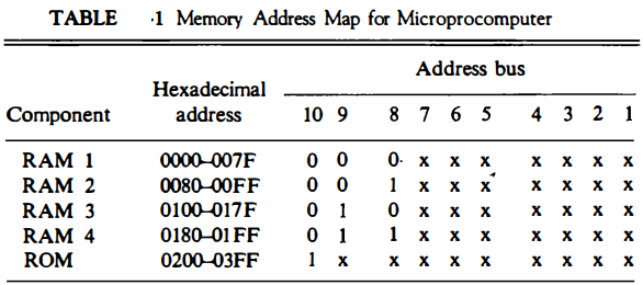
The component column specifies whether a RAM or a ROM chip is used. The hexadecimal address column assigns a range of hexadecimal equivalent addresses for each chip.
The address bus lines are listed in the third column. Although there are 16 lines in the address bus, the table shows only 10 lines because the other 6 are not used in this example and are assumed to be zero.
The small x'sunder the address bus lines designate those lines that must be connected to the address inputs in each chip. The RAM chips have 128 bytes and need seven address lines.
The ROM chip has 512 bytes and needs 9 address lines. The x's are always assigned to the low-order bus lines: lines 1 through 7 for the RAM and lines 1 through 9 for the ROM.
It is now necessary to distinguish between four RAM chips by assigning to each a different address. For this particular example we choose bus lines 8 and 9 to represent four distinct binary combinations.
Note that any other pair of unused bus lines can be chosen for this purpose. The table clearly shows that the nine low-order bus lines constitute a memory space for RAM equal to 29 = 512 bytes.
The distinction between a RAM and ROM address is done with another bus line. Here we choose line 10 for this purpose. When line 10 is 0, the CPU selects a RAM, and when this line is equal to 1, it selects the ROM.
The equivalent hexadecimal address for each chip is obtained from the information under the address bus assignment. The address bus lines are subdivided into groups of four bits each so that each group can be represented with a hexadecimal digit.
The first hexadecimal digit represents lines 13 to 16 and is always 0. The next hexadecimal digit represents lines 9 to 12, but lines 11 and 12 are always 0.
The range of hexadecimal addresses for each component is determined from the x's associated with it. These x's represent a binary number that can range from an all-0's to an all-1's value.
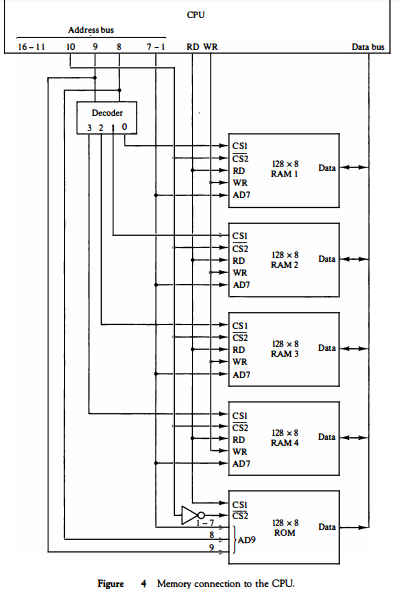
Memory Connection to CPU
RAM and ROM chips are connected to a CPU through the data and address buses.
The low-order lines in the address bus select the byte within the chips and other lines in the address bus select a particular chip through its chip select inputs.
The connection of memory chips to the CPU is shown in Fig. 4. This configuration gives a memory capacity of 512 bytes of RAM and 512 bytes of ROM. It implements the memory map of Table 1. Each RAM receives the seven low-order bits of the address bus to select one of 128 possible bytes.
The particular RAM chip selected is determined from lines 8 and 9 in the address bus. This is done through a 2 x 4 decoder whose outputs go to the CS1 inputs in each RAM chip.
Thus, when address lines 8 and 9 are equal to 00, the first RAM chip is selected. When 01, the second RAM chip is selected, and so on. The RD and WR outputs from the microprocessor are applied to the inputs of each RAM chip.
The selection between RAM and ROM is achieved through bus line 10. The RAMs are selected when the bit in this line is 0, and the ROM when the bit is 1.
The other chip select input in the ROM is connected to the RD control line for the ROM chip to be enabled only during a read operation. Address bus lines 1 to 9 are applied to the input address of ROM without going through the decoder.
This assigns addresses 0 to 511 to RAM and 512 to 1023 to ROM. The data bus of the ROM has only an output capability, whereas the data bus connected to the RAMs can transfer information in both directions .
The example just shown gives an indication of the interconnection complexity that can exist between memory chips and the CPU.
The more chips that are connected, the more external decoders are required for selection among the chips . The designer must establish a memory map that assigns addresses to the various chips from which the required connections are determined.
Auxiliary Memory
The most common auxiliary memory devices used in computer systems are magnetic disks and tapes. Other components used, but not as frequently, are magnetic drums, magnetic bubble memory, and optical disks.
To understand fully the physical mechanism of auxiliary memory devices one must have a knowledge of magnetics, electronics, and electromechanical systems.
Although the physical properties of these storage devices can be quite complex, their logical properties can be characterized and compared by a few parameters. The important characteristics of any deviceare its access mode, access time, transfer rate, capacity, and cost.
The average time required to reach a storage location in memory and obtain its contents is called the access time.
In electromechanical devices with moving parts such as disks and tapes, the access time consists of a seek time required to position the read-write head to a location and a transfer time required to transfer data to or from the device. Because the seek time is usually much longer than the transfer time, auxiliary storage is organized in records or blocks.
A record is a specified number of characters or words. Reading or writing is always done on entire records. The transfer rate is the number of characters or words that the device can transfer per second, after it has been positioned at the beginning of the record.
Magnetic drums and disks are quite similar in operation. Both consist of high-speed rotating surfaces coated with a magnetic recording medium. The rotating surface of the drum is a cylinder and that of the disk, a round flat plate.
The recording surface rotates at uniform speed and is not started or stopped during access operations. Bits are recorded as magnetic spots on the surface as it passes a stationary mechanism called a write head.
Stored bits are detected by a change in magnetic field produced by a recorded spot on the surface as it passes through a read head. The amount of surface available for recording in a disk is greater than in a drum of equal physical size.
Therefore, more information can be stored on a disk than on a drum of comparable size. For this reason, disks have replaced drums in more recent computers.
Magnetic Disks
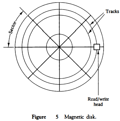
A magnetic disk is a circular plate constructed of metal or plastic coated with magnetized material. Often both sides of the disk are used and several disks may be stacked on one spindle with read/write heads available on each surface.
All disks rotate together at high speed and are not stopped or started for access purposes. Bits are stored in the magnetized surface in spots along concentric circles called tracks.
The tracks are commonly divided into sections called sectors. In most systems, the minimum quantity of information which can be transferred is a sector. The subdivision of one disk surface into tracks and sectors is shown in Fig. 5.
Some units use a single read/write head for each disk surface. In this type of unit, the track address bits are used by a mechanical assembly to move the head into the specified track position before reading or writing.
In other disk systems, separate read/write heads are provided for each track in each surface. The address bits can then select a particular track electronically through a decoder circuit.
This type of unit is more expensive and is found only in very large computer systems. Permanent timing tracks are used in disks to synchronize the bits and recognize the sectors.
A disk system is addressed by address bits that specify the disk number, the disk surface, the sector number and the track within the sector. After the read/write heads are positioned in the specified track, the system has to wait until the rotating disk reaches the specified sector under the read/write head.
Information transfer is very fast once the beginning of a sector has been reached. Disks may have multiple heads and simultaneous transfer of bits from several tracks at the same time.
A track in a given sector near the circumference is longer than a track near the center of the disk If bits are recorded with equal density, some tracks will contain more recorded bits than others.
To make all the records in a sector of equal length, some disks use a variable recording density with higher density on tracks near the center than on tracks near the circumference. This equalizes the number of bits on all tracks of a given sector.
Disks that are permanently attached to the unit assembly and cannot be removed by the occasional user are called hard disks. A disk drive with removable disks is called a floppy disk. The disks used with a floppy disk drive are small removable disks made of plastic coated with magnetic recording material.
There are two sizes commonly used, with diameters of 5.25 and 3. 5 inches. The 3.5-inch disks are smaller and can store more data than can the 5.25-inch disks.
Floppy disks are extensively used in personal computers as a medium for distributing software to computer users.
Magnetic Tape
A magnetic tape transport consists of the electrical, mechanical, and electronic components to provide the parts and control mechanism for a magnetic-tape unit.
The tape itself is a strip of plastic coated with a magnetic recording medium. Bits are recorded as magnetic spots on the tape along several tracks.
Usually, seven or nine bits are recorded simultaneously to form a character together with a parity bit. Read/write heads are mounted one in each track so that data can be recorded and read as a sequence of characters.
Magnetic tape units can be stopped, started to move forward or in reverse, or can be rewound.
However, they cannot be started or stopped fast enough between individual characters.
For this reason, information is recorded in blocks referred to as records. Gaps of unrecorded tape are inserted between records where the tape can be stopped.
The tape starts moving while in a gap and attains its constant speed by the time it reaches the next record. Each record on tape has an identification bit pattern at the beginning and end.
By reading the bit pattern at the beginning, the tape control identifies the record number.
By reading the bit pattern at the end of the record, the control recognizes the beginning of a gap.
A tape unit is addressed by specifying the record number and the number of characters in the record. Records may be of fixed or variable length.
Associative Memory
Many data-processing applications require the search of items in a table stored in memory.
An assembler program searches the symbol address table in order to extract the symbol's binary equivalent.
An account number may be searched in a file to determine the holder's name and account status.
The established way to search a table is to store all items where they can be addressed in sequence.
The search procedure is a strategy for choosing a sequence of addresses, reading the content of memory at each address, and comparing the information read with the item being searched until a match occurs.
The number of accesses to memory depends on the location of the item and the efficiency of the search algorithm.
Many search algorithms have been developed to minimize the number of accesses while searching for an item in a random or sequential access memory.
The time required to find an item stored in memory can be reduced considerably if stored data can be identified for access by the content of the data itself rather than by an address.
A memory unit accessed by content is called an associative memory or content addressable memory (CAM).
This type of memory is accessed simultaneously and in parallel on the basis of data content rather than by specific address or location. When a word is written in an associative memory, no address is given.
The memory is capable of finding an empty unused location to store the word.
When a word is to be read from an associative memory, the content of the word, or part of the word, is specified.
The memory locates all words which match the specified content and marks them for reading.
Because of its organization, the associative memory is uniquely suited to do parallel searches by data association. Moreover, searches can be done on an entire word or on a specific field within a word.
An associative memory is more expensive than a random access memory because each cell must have storage capability as well as logic circuits for matching its content with an external argument.
For this reason, associative memories are used in applications where the search time is very critical and must be very short.
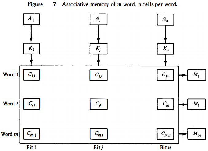
Hardware Organization
The block diagram of an associative memory is shown in Fig. 6. It consists of a memory array and logic for m words with n bits per word. The argument register A and key register K each have n bits, one for each bit of a word.
The match register M has m bits, one for each memory word. Each word in memory is compared in parallel with the content of the argument register. The words that match the bits of the argument register set a corresponding bit in the match register.
After the matching process, those bits in the match register that have been set indicate the fact that their corresponding words have been matched.
Reading is accomplished by a sequential access to memory for those words whose corresponding bits in the match register have been set.
The key register provides a mask for choosing a particular field or key in the argument word.
The entire argument is compared with each memory word if the key register contains all 1's.
Otherwise, only those bits in the argument that have 1's in their corresponding position of the key register are compared.
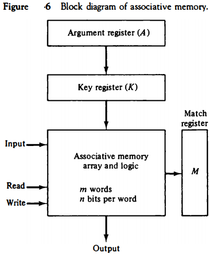
Thus the key provides a mask or identifying piece of information which specifies how the reference to memory is made. To illustrate with a numerical example, suppose that the argument register A and the key register K have the bit configuration shown below. Only the three leftmost bits of A are compared with memory words because K has 1's in these positions.
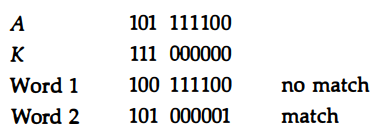
Word 2 matches the unmasked argument field because the three leftmost bits of the argument and the word are equal.
The relation between the memory array and external registers in an associative memory is shown in Fig. 7.
The cells in the array are marked by the letter C with two subcripts. The first subscript gives the word number and the second specifies the bit position in the word.
Thus cell Cij is the cell for bit j in word i. A bit Aj in the argument register is compared with all the bits in column j of the array provided that Kj = 1.
This is done for all columns j = 1, 2, . . . , n. If a match occurs between all the unmasked bits of the argument and the bits in word i, the corresponding bit Mi in the match register is set to 1.
If one or more unmasked bits of the argument and the word do not match, Mi is cleared to 0.