STORAGE ELEMENTS : FLIP FLOPS
The state of a latch or flip-flop is switched by a change in the control input. This momentary change is called a trigger and the transition it causes is said to trigger the flip-flop.
The D-latch with pulses in its control input is essentially a flip-flop that is triggered every time the pulse goes to the logic-1 level.
A sequential circuit has a feedback path from the outputs of the flip-flop to the input of the combinational circuit. Consequently the inputs of the flip-flops are derived in part from the outputs of the same and other flip-flops.
Flip-flop circuits are constructed in such a way as to make them operate properly when they are part of a sequential circuit that employs a common clock. The problem with the latch is that it responds to a change in the level of a clock pulse.
A positive level response in the enable input allows changes in the output when the D input changes while the clock pulse stays at logic 1. The key to the proper operation of a flip-flop is to trigger it only during a signal transition.
There are two ways that a latch can be modified to form a flip-flop .
Employ two latches in a special configuration that isolates the output of the flip-flop and prevents it from being affected while the input to the flip-flop is changing.
To produce a flip- flop that triggers only during a signal transition (from 0 to 1 or from 1 to 0) of the synchronizing signal (clock) and is disabled during the rest of the clock pulse.
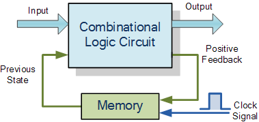
Edge-Triggered D Flip-Flop
The construction of a D flip-flop with two D latches and an inverter is such that the first latch is called the master and the second the slave.
The circuit samples the D input and changes its output Q only at the negative edge of the synchronizing or controlling clock (designated as Clk).
Working of the Edge-Triggered D Flip-Flop
When the clock is 0, the output of the inverter is 1. The slave latch is enabled and its output Q is equal to the master output 'Y'. The master latch is disabled because Clk = 0.
When the input pulse changes to the logic-1 level, the data from the external D input are transferred to the master. The slave however is disabled as long as the clock remains, at the 1 level because its enable input is equal to 0.
Any change in the input changes the master output at Y but cannot affect the slave output.
When the clock pulse returns to 0 the master is disabled and is isolated from the D input. At the same time the slave is enabled and the value of Y is transferred to the output of the flip-flop at Q. Thus a change in the output of the flip-flop can be triggered only by and during the transition of the clock from 1 to 0.
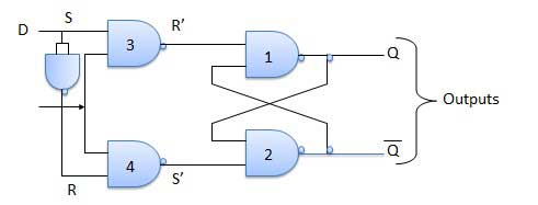
Circuit diagram of Edge-Triggered D Flip-Flop :
Block diagram of Edge-Triggered D Flip-Flop :
Truth Table of Edge-Triggered D Flip-Flop :
Operation of Edge-Triggered D Flip-Flop :

| Input | Output | Comments | |||
|---|---|---|---|---|---|
| E | D | Q(n+1) | Q(n+1) | ||
| 1 | 0 | 0 | 1 | Reset | |
| 1 | 1 | 1 | 0 | Set | |
| Sr No |
Condition | Operation |
|---|---|---|
| 1 | E = 0 |
Latch is disabled. Hence no change in output. |
| 2 | E = 1 and D = 0 |
If E = 1 and D = 0 then,S = 0 and R = 1. Hence irrespective of the present state, the next state is Qn+1 = 0 and Qn+1 = 1. This is the reset condition. |
| E = 1 and D = 1 |
If E = 1 and D = 1, then,S = 1 and R = 0. This will set the latch and Qn+1 = 1 and Qn+1 = 0 irrespective of the present state. |
The behavior of the master - slave flip-flop:
The output may change only once
A Change in the output is triggered by the negative edge of the clock
The change may occur only during the clock's negative level.
The value that is produced at the output of the flip-flop is the value that was stored in the master stage immediately before the negative edge occurred.
It is also possible to design the circuit so that the flip-flop output changes on the positive edge of the clock.
This happens in a flip-flop that has an additional inverter between the Clk terminal and the junction between the other inverter and input En of the master latch. Such a flip-flop is triggered with a negative pulse, so that the negative edge of the clock affects the master and the positive edge affects the slave and the output terminal.
In sum when the input clock in the positive-edge-triggered flip-flop makes a positive transition the value of D is transferred to Q. A negative transition of the clock (i.e. from 1 to 0 ) does not affect the output nor is the output affected by changes in D when Clk is in the steady logic-1 level or the logic-0 level. Hence, this type of flip-flop responds to the transition from 0 to 1 and nothing else.
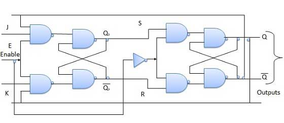
Circuit diagram of master - slave flip-flop :
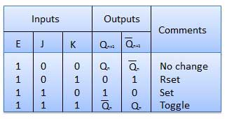
Truth table of master - slave flip-flop :
Operation of master - slave flip-flop :

| Sr No |
Condition | Operation |
|---|---|---|
| 1 | J = K = 0 (No change) | When clock = 0, the slave becomes active and master is inactive. But since the S and R inputs have not changed, the slave outputs will also remain unchanged. Therefore outputs will not change if J = K =0. |
| 2 | J = 0 and K = 1 (Reset) | Clock = 1 −> Master is active, slave is inactive. Therefore outputs of the master become Q1 = 0 and Q1 = 1. That means S = 0 and R = 1 Clock = 0 then we have Slave active and master inactive. Therefore outputs of the slave become Q1 = 0 and Q1 = 1. Again at clock = 1 − Master is active, slave isinactive. Therefore even with the changed outputs Q1 = 0 and Q1 = 1 fed back to master, its output will be Q1 = 0 and Q1 = 1. That,means S = 0 and R = 1.,Hence with clock = 0 and,slave becoming active the outputs of slave will remain Q1 = 0 and Q1 = 1.,Thus we get a stable output from the Master slave. |
| 3 | J = 1 and K = 0,(Set) | Clock = 1 − Master active, slave inactive. Therefore outputs of the master become Q1 = 1 and Q1 = 0. That means S = 1 and R =0.,Clock = 0 − Slave active, master inactive. Therefore outputs of the slave become Q1 = 1 and Q1 = 0. Again clock = 1 − then it can be shown that the outputs of the slave are stabilized to Q1 = 1 and Q1 = 0. |
| 4 | J = K = 1,(Toggle) | Clock = 1 − Master,active, slave inactive. Outputs of master will toggle. So S and R also will,be inverted. Clock = 0 − Slave,active, master inactive. Outputs of slave will toggle. These changed output are,returned back to the master inputs. But since clock = 0, the master is still,inactive. So it does not respond to these changed outputs. This avoids the,multiple toggling which leads to the race around condition. The master slave,flip flop will avoid the race around condition. |
Edge-Triggered flip-flop using SR latches
Two latches respond to the external D (data) and Clk (clock) inputs.
The third latch provides the: output for the flip-flop. The S and R inputs of the output latch are maintained at the logic-1 level when Clk = 0. This causes the output to remain in the present state.
When the clock becomes 1 and input D = 0, R changes to 0. This causes the flip-flop to go to the reset state making Q = 0.
If there is a change in the D input while Clk = 1, terminal R remains at 0 because Q is 0, Thus the flip-flop is locked out and is unresponsive to further changes in the input.
When the clock returns to 0, R goes to 1, placing the output latch in the quiescent condition without changing the output.
Similarly, if D = 1 when Clk goes from 0 to 1, S changes to 0, This causes the circuit to go to the set state, making Q = 1. Any change in D while Clk = 1 does not affect the output
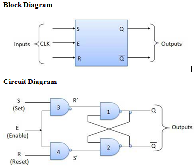
Truth table of Edge-Triggered flip-flop using SR latches :
Operation of Edge-Triggered flip-flop using SR latches :
| Inputs | Outputs | Comments | ||||
|---|---|---|---|---|---|---|
| E | S | R | Qn+1 | Qn+1 | ||
| 1 | 0 | 0 | Qn | Qn | no change |
|
| 1 | 0 | 1 | 0 | 1 | reset | |
| 1 | 1 | 0 | 1 | 0 | set | |
| 1 | 1 | 1 | x | x | indeterminate | |
| No. | Condition | Operation |
|---|---|---|
| 1 | S = R = 0 : No change | If S = R = 0 then output of NAND gates 3 and 4 are forced to become 1. Hence R' and S' both will be equal to 1. Since S' and R' are the input of the basic S-R latch using NAND gates, there will be no change in the state of outputs. |
| 2 | S = 0, R = 1, E = 1 | Since S = 0, output of NAND-3 i.e. R' = 1 and E = 1 the output of NAND-4 i.e. S' = 0. Hence Qn+1 = 0 and Q'n+1 = 1. This is reset condition. |
| 3 | S = 1, R = 0, E = 1 | Output of NAND-3 i.e. R' = 0 and output of NAND-4 i.e. S' = 1. Hence output of S-R NAND latch is Qn+1 = 1 and Q'n+1 = 0. This is the reset condition. |
| 4 | S = 1, R = 1, E = 1 | As S = 1, R = 1 and E = 1, the output of NAND gates 3 and 4 both are 0 i.e. S' = R' = 0. Hence the Race condition will occur in the basic NAND latch. |
Other Flip-Flops
The most economical and efficient flip-flop constructed in this manner is the edge-triggered D flip-flop because it requires the smallest number of gates.
Other types of flip-flops can be constructed by using the D flip-flop and external logic. Two flip-flops less widely used in the design of digital systems are the JK and T flip-flops.
There are three operations that can be performed with a flip-flop: Set it to 1, reset it to 0 Or complement its output.
J-K Flip Flop
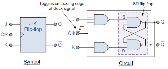
The J inputs sets the flip-flop to 1, the K input resets it to 0 and when both inputs are enabled the output is complemented.
Operation of a JK Flip-Flop:
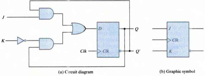
Circuit applied to input D: D = JQ' + K'Q
When J = 1, k = 0, D = Q' + Q = 1, so the next clock edge sets the output to 1.
When J = 0, k = 1, D = 0, so the next clock edge resets the output to 0.
When J = K = 1, D = Q', so the next clock edge complements the output.
When J = K = 0, D = Q, so the next clock edge leaves the output unchanged.
Circuit diagram of J-K Flip Flop :
Truth table J-K Flip Flop :
| Input | Output | Description | |||
|---|---|---|---|---|---|
| J | K | Q | Qn+1 | ||
| Same as SR latch |
0 | 0 | 0 | 0 | Memory no change |
| 0 | 0 | 0 | 1 | ||
| 0 | 1 | 1 | 0 | Reset Q to 0 |
|
| 0 | 1 | 0 | 1 | ||
| 1 | 0 | 0 | 1 | Set Q to 1 |
|
| 1 | 0 | 1 | 0 | ||
| Toggle Action |
1 | 1 | 0 | 1 | Toggle |
| 1 | 1 | 1 | 0 | ||
T (toggle) flip - flop
The T (toggle) flip flop is a complementing flip-flop and can be obtained from a JK flip flop when inputs J and K are tied together.
When T = 0 ( J = K = 0), a clock edge does not change the output
When T = 1 (J = K = 1 ) a clock edge complements the Output. The complementing flip-flop is useful for designing binary counters
The T flip-flop can be constructed with a D flip-flop and an exclusive-OR gate as shown below:

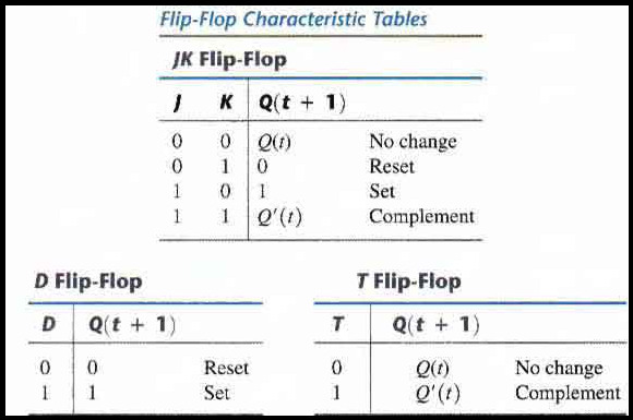
Characteristic Tables - JK Flipflop
A characteristic table defines the logical properties of a flip-flop by describing its operation in tabular form.
They define the next state (i.e. the state that results from a clock transition) as a function of the inputs and the present state. Q(t) refers to the present state (i.e. the state present prior to the application of a clock edge). Q(t + 1) is the next state one clock period later.
Note that the clock edge input is not included in the characteristic table but is implied to occur between times t and t + 1.
Thus, Q(t) denotes the state of the flip-flop immediately before the clock edge and Q(t + 1) denotes the state that results from the clock transition.
The characteristic table for the J K flip-flop shows that the next state is equal to the present state when inputs J and K are both equal to 0. This condition can be expressed as Q(t + 1) = Q(t) indicating that the clock produces no change of state.
When K = 1, J = 0 the clock resets the flip-flop and Q(t + 1) = 0
With J = 1 and K = 0 the flip-flop sets and Q(t + 1) = 1
When both J and K are equal to 1 the next state ,changes to the complement of the present state, a transition that can be expressed as Q(t + 1) = Q'(t).
The logical properties of JK flip-flop, as described in the characteristic table can be expressed algebraically with a characteristic equation. Which is : Q(t + 1) = JQ' + K'Q
Characteristic Tables - D FlipFlop
The next state of the D flipflop is dependent only on the D input and is independent of the present state. This can be expressed as Q(t+1) = D.
It means that the next state value is equal to the value of D. Note that the D flip-flop does not have a "no-change" condition. Such a condition can be accomplished either by disabling the clock or by operating the clock by having the output of the flip-flop connected into the D input.
Either method effectively circulates the output of the flip-flop when the state of the flip- flop must remain unchanged.
The logical properties of D flip-flop, as described in the characteristic table can be expressed algebraically with a characteristic equation. Which is : Q(t + 1) = D
Characteristic Tables - T Flip Flop
The characteristic table of the T flip-flop has only two conditions When T = 0 the clock edge does not change the state: when T = 1, the clock edge complements the state of the flip - flop
The logical properties of T flip-flop, as described in the characteristic table can be expressed algebraically with a characteristic equation which is : Q(t + 1) = TQ' + T'Q